bipolar transistor control. The difference between a field effect transistor and a bipolar one. Scope of their application
In the following articles there will be devices that must manage external loads. By external load, I mean everything that is attached to the legs of the microcontroller - LEDs, light bulbs, relays, motors, actuators ... well, you understand. And no matter how hackneyed this topic is, but in order to avoid repetition in the following articles, I still risk not being original - you will forgive me :). I briefly recommendation form, I will show the most common ways to connect the load (if you want to add something, I will only be happy).
Let's agree right away that we are talking about a digital signal (the microcontroller is still a digital device) and we will not deviate from the general logic: 1
- included, 0
-turned off. Let's start.
load direct current are: LEDs, lamps, relays, DC motors, servo drives, various actuators, etc. Such a load is most simply (and most often) connected to the microcontroller.
1.1 Connection loads through a resistor.
The simplest and probably the most commonly used method when it comes to LEDs.
The resistor is needed in order to limit the current flowing through the leg of the microcontroller to acceptable 20mA. It is called ballast or extinguishing. You can roughly calculate the value of the resistor knowing the load resistance Rn.
Rextinguishing =(5v / 0.02A) - Rн = 250 - Rn
As you can see, even in the worst case, when the load resistance is zero, 250 ohms is enough to ensure that the current does not exceed 20mA. So, if you don’t feel like counting something there, put 300 ohm and you will protect the port from overload. The advantage of the method is obvious - simplicity.
1.2 Connection loads using a bipolar transistor.
If it so happened that your load consumes more than 20mA, then, of course, a resistor will not help here. You need to somehow increase (read amplify) the current. What is used to amplify the signal? Correctly. Transistor!

For reinforcement it is more convenient to apply n-p-n transistor connected in a circuit OE. With this method, you can connect a load with a higher supply voltage than the power supply of the microcontroller. The base resistor is a limiting resistor. It can vary over a wide range (1-10 kOhm), in any case, the transistor will operate in saturation mode. The transistor can be any n-p-n transistor. Gain is practically irrelevant. The transistor is selected according to the collector current (the current we need) and the collector-emitter voltage (the voltage that powers the load). Power dissipation also matters - so as not to overheat.
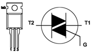
Of the common and easily accessible ones, you can use BC546, BC547, BC548, BC549 with any letters (100mA), and the same KT315 will do (it’s from someone left with old stocks).
- Datasheet for bipolar transistor BC547
1.3 Connection loads using a field effect transistor.
Well, if the current of our load lies within a dozen amperes? A bipolar transistor cannot be used, since the control currents of such a transistor are large and most likely will exceed 20mA. The output can be either a composite transistor (read below) or a field effect transistor (aka MOS, aka MOSFET). The field effect transistor is just a wonderful thing, since it is not controlled by current, but by the potential at the gate. This makes it possible for the microscopic gate current to drive large load currents.
Any n-channel field-effect transistor will do for us. We choose, like bipolar, by current, voltage and power dissipation.

When you turn on the field effect transistor, you need to consider a number of points:
- since the gate, in fact, is a capacitor, then at the moments of switching of the transistor, large currents flow through it (for a short time). In order to limit these currents, a limiting resistor is placed in the gate.
- the transistor is controlled by low currents, and if the output of the microcontroller to which the gate is connected is in a high-impedance Z-state, the field switch will open and close unpredictably, catching interference. To eliminate this behavior, the leg of the microcontroller must be “pressed” to the ground with a resistor of the order of 10 kOhm.
The field-effect transistor, against the background of all its positive qualities, has a drawback. The price to pay for low current control is the slowness of the transistor. PWM, of course, it will pull, but it will answer you with overheating if the permissible frequency is exceeded.
1.4 Connection loads using a composite Darlington transistor.
An alternative to using a FET for high current loads is to use a compound Darlington transistor. Outwardly, this is the same transistor as, say, a bipolar one, but inside, a preliminary amplifying circuit is used to control a powerful output transistor. This allows small currents to control a powerful load. The application of the Darlington transistor is not as interesting as the application of the assembly of such transistors. There is such a wonderful chip as ULN2003. It contains as many as 7 Darlington transistors, and each can be loaded with current up to 500mA, and they can be connected in parallel to increase the current.
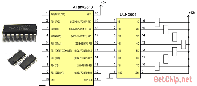
The microcircuit is very easy to connect to the microcontroller (just a leg to a leg) has a convenient wiring (input opposite the output) and does not require additional strapping. As a result of this successful design, the ULN2003 is widely used in amateur radio practice. Accordingly, it will not be difficult to get it.
- Datasheet for assembly Darlington ULN2003
If you need to manage devices alternating current(most often 220v), then everything is more complicated, but not by much.
2.1 Connection loads using a relay.
The simplest and probably the most reliable is the connection using a relay. The relay coil, by itself, is a high-current load, so you can’t turn it on directly to the microcontroller. The relay can be connected through a field or bipolar transistor or through the same ULN2003 if you need several channels.

The advantages of this method are large switched current (depending on the selected relay), galvanic isolation. Disadvantages: limited speed / frequency of switching on and mechanical wear of parts.
It makes no sense to recommend something for use - there are a lot of relays, choose according to the necessary parameters and price.
2.2 Connection loads using a triac (triac).
If you need to control a powerful AC load, and especially if you need to control the power delivered to the load (dimers), then you simply cannot do without the use of a triac (or triac). The triac opens with a short current pulse through the control electrode (for both negative and positive voltage half-waves). The triac closes itself, at the moment of the absence of voltage on it (when the voltage passes through zero). This is where the difficulties begin. The microcontroller must control the moment of transition through zero voltage and, at a precisely defined moment, give a pulse to open the triac - this is the constant employment of the controller. Another difficulty is the lack of galvanic isolation in the triac. You have to do it on separate elements, complicating the circuit.
Although modern triacs are driven by a fairly low current and can be connected directly (through a limiting resistor) to the microcontroller, for safety reasons they have to be connected through optical isolators. And this applies not only to the triac control circuits, but also to the zero control circuits. 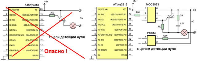
A rather ambiguous way to connect the load. Since, on the one hand, it requires the active participation of the microcontroller and a relatively complex circuit design solution. On the other hand, it allows very flexible manipulation of the load. Another disadvantage of using triacs is the large amount of digital noise generated during their operation - suppression circuits are needed.
Triacs are quite widely used, and in some areas are simply irreplaceable, so getting them is not a problem. Very often triacs of the BT138 type are used in amateur radio.
Hello dear readers. In this article, we will consider the difference between a field-effect transistor and a bipolar one, and find out in which areas both transistors are used.
So, let's begin…
Among semiconductor devices, there are two large groups, which include field and bipolar. They are widely used in electronics and radio engineering as generators, amplifiers and converters. electrical signals. To understand the main difference between these devices, it is necessary to consider them in more detail.
Bipolar transistors
The conductive area of the structure consists of three “soldered” semiconductor parts, alternating according to the type of conductivity. A semiconductor with donor (electronic) conductivity is designated as n-type, with acceptor (hole) - p-type. Thus, we can observe only two variants of alternation - p-n-p, or n-p-n. On this basis, bipolar transistors with n-p-n and p-n-p structures are distinguished.
The common part of a transistor crystal in contact with the other two is called the "base". The other two are "collector" and "emitter". The degree of saturation of the base with charge carriers (electrons or electron vacancies "holes") determines the degree of conductivity of the entire transistor crystal. Thus, the conductivity of the transistor transitions is controlled, which makes it possible to use it as an element of signal power amplification, or a key.
FETs
The conductive part of the structure is a p- or n-type semiconductor channel in metal. The load current flows through the channel through the electrodes called "drain" and "source". The cross section of the conducting channel and its resistance depends on reverse voltage at the pn junction of the metal-semiconductor interface of the channel. The control electrode connected to the metal area is called the gate.
The field-effect transistor channel can have an electrical connection with the gate metal - an uninsulated gate, or it can be separated from it by a thin layer of dielectric - an insulated gate.
Which transistors are better field or bipolar?
And so, we learned that the main difference between these two types of transistors is control. Let's look at other advantages of field-effect transistors compared to bipolar ones:
- high input impedance for direct current and at high frequency, hence low control losses
- high speed (due to the absence of accumulation and resorption of minor carriers)
- almost complete electrical decoupling of the input and output circuits, low throughput capacitance since the amplifying properties of field-effect transistors are due to the transfer of the main charge carriers, their upper limit of effective amplification is higher than that of bipolar
- quadratic volt - ampere characteristic(similar to triode)
- high temperature stability
- low noise level, since field-effect transistors do not use the phenomenon of injection of minor charge carriers, which makes bipolar transistors “noisy”
- low power consumption
The accumulation and resorption of minority charge carriers is absent in field-effect transistors, which is why their speed is very high (as noted by the developers of power equipment). And since the transferred main charge carriers are responsible for amplification in field-effect transistors, the upper limit of effective amplification for field-effect transistors is higher than for bipolar ones.
Here we also note the high temperature stability, a low level of interference (due to the absence of injection of minority charge carriers, as occurs in bipolar ones), and efficiency in terms of energy consumption.
Current or field, transistor control
For most people who deal with electronics in one way or another, the fundamental structure of field-effect and bipolar transistors should be known. At least from the name "field effect transistor", it is obvious that it is controlled by a field, the electric field of the gate, while the bipolar transistor is controlled by the base current.
Current and field, the difference here is cardinal. For bipolar transistors, the collector current is controlled by changing the base control current, while to control the drain current of a field-effect transistor, it is enough to change the voltage applied between the gate and the source, and no control current as such is needed.
Different reaction to heat
For bipolar transistors, the collector-emitter temperature coefficient of resistance is negative (that is, with increasing temperature, the resistance decreases and the collector-emitter current increases). For field-effect transistors, the opposite is true - the drain-source temperature coefficient is positive (with increasing temperature, the resistance increases, and the drain-source current decreases).
An important consequence of this fact is that if bipolar transistors cannot just be connected in parallel (for the purpose of amplification), without current-leveling resistors in the emitter circuit, then with field-effect transistors everything is much simpler - thanks to the auto-balancing of the drain-source current when the load / heating changes - they can be freely turned on parallel without equalizing resistors. This is related to temperature properties p-n junction and a simple p- or n-type semiconductor. For this reason, field-effect transistors are much less likely to experience irreversible output thermal breakdown than bipolar ones.
So, to achieve high switching currents, you can easily dial a composite key from several parallel field-effect transistors, which is used in many places in practice, for example, in inverters.
But bipolar transistors cannot be simply paralleled, they need current-leveling resistors in emitter circuits. Otherwise, due to an imbalance in a powerful composite key, one of the bipolar transistors will sooner or later have an irreversible thermal breakdown. Field composite keys are almost not threatened by this problem. These characteristic thermal features are associated with the properties of a simple n- and p-channel and p-n junction which are drastically different.
Scopes of those and other transistors
The differences between field and bipolar transistors clearly separate their areas of application. For example, in digital circuits, where a minimum current consumption in the standby state is required, field-effect transistors are used much more widely today. In analog microcircuits, field-effect transistors help to achieve high linearity of the amplifying characteristic in a wide range of supply voltages and output parameters.
Reel-to-reel circuits are conveniently implemented today with field-effect transistors, because it is easy to achieve the swing of the output voltages as signals for the inputs, coinciding almost with the supply voltage level of the circuit. Such circuits can simply connect the output of one to the input of another, and no voltage limiters or resistor dividers are needed.
As for bipolar transistors, their typical applications remain: amplifiers, their cascades, modulators, detectors, logic inverters and transistor logic microcircuits.
Field win, why?
Prominent examples of field-effect transistor devices are wristwatches and TV remote controls. Due to the use of CMOS structures, these devices can operate for up to several years from one miniature power source - batteries or accumulators, because they practically do not consume energy.
Currently, field-effect transistors are increasingly being used in various radio devices, where they are already successfully replacing bipolar ones. Their use in radio transmitting devices makes it possible to increase the frequency of the carrier signal, providing such devices with high noise immunity.
Possessing low resistance in the open state, they are used in the final stages of power amplifiers audio frequencies high power (Hi-Fi), where, again, bipolar transistors and even vacuum tubes are successfully replaced.
In high power devices, such as devices soft start motors, insulated gate bipolar transistors (IGBT) - devices that combine both bipolar and field-effect transistors are already successfully replacing thyristors.
Video, the difference between a field-effect transistor and a bipolar one
06 Jan 2017
In practice, it often becomes necessary to control some powerful electrical device using a digital circuit (for example, a microcontroller). It can be a powerful LED that consumes a large current, or a device powered by a 220 V network. Let's consider typical solutions to this problem.
Types of management
Conventionally, 3 groups of methods can be distinguished:
- DC load control.
- Transistor key on a bipolar transistor.
- Transistor key on a MOSFET (MOSFET).
- Transistor key on IGBT.
- AC load control.
- thyristor key.
- Simistor key.
- Universal method.
- Relay.
The choice of control method depends both on the type of load and on the type of digital logic used. If the circuit is built on TTL microcircuits, then it should be remembered that they are controlled by current, in contrast to CMOS, where control is carried out by voltage. Sometimes it matters.
Bipolar transistor switch
For the current $I_(LED) = 0(,)075\,A$, the control current must be $\beta = 50$ times less:
Let us take the voltage drop at the emitter-base junction equal to $V_(EB) = 0(,)7\,V$.
The resistance was rounded down to provide current headroom.
Thus, we have found the values of the resistances R1 and R2.
Darlington transistor
If the load is very powerful, then the current through it can reach several amperes. For high power transistors, the $\beta$ factor may be insufficient. (Moreover, as can be seen from the table, for powerful transistors it is already small.)
In this case, you can use a cascade of two transistors. The first transistor controls the current, which turns on the second transistor. Such a switching circuit is called a Darlington circuit.

In this circuit, the $\beta$ coefficients of the two transistors are multiplied, which makes it possible to obtain a very large current transfer coefficient.
To increase the turn-off speed of transistors, you can connect the emitter and base with a resistor for each.
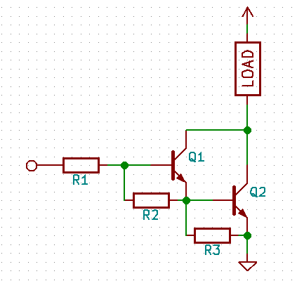
The resistances must be large enough not to affect the base-emitter current. Typical values are 5…10 kΩ for voltages of 5…12 V.
Darlington transistors are available as a separate device. Examples of such transistors are given in the table.
Otherwise, the operation of the key remains the same.
FET key
In the future, we will call the field effect transistor specifically MOSFET, that is, insulated gate field effect transistors (they are also MOS, they are also MIS). They are convenient in that they are controlled exclusively by voltage: if the voltage at the gate is greater than the threshold, then the transistor opens. In this case, the control current does not flow through the transistor while it is open or closed. This is a significant advantage over bipolar transistors, in which current flows all the time the transistor is on.
Also, in the future, we will only use n-channel MOSFETs (even for push-pull circuits). This is because n-channel transistors are cheaper and have better performance.
The simplest MOSFET switch circuit is shown below.

Again, the load is connected "from above", to the drain. If you connect it "from below", then the circuit will not work. The fact is that the transistor opens if the voltage between the gate and the source exceeds the threshold. When connected "from below", the load will give an additional voltage drop, and the transistor may not open or open incompletely.
With push-pull control, the capacitor discharge circuit forms, in fact, an RC circuit in which maximum current discharge will be equal to
where $V$ is the voltage that controls the transistor.
Thus, it will be enough to put a 100 ohm resistor in order to limit the charge-discharge current to 10 mA. But the greater the resistance of the resistor, the slower it will open and close, since the time constant $\tau = RC$ will increase. This is important if the transistor switches frequently. For example, in a PWM controller.
The main parameters that you should pay attention to are the threshold voltage $V_(th)$, the maximum current through the drain $I_D$ and the drain-source resistance $R_(DS)$ of an open transistor.
Below is a table with examples of characteristics of MOSFETs.
| Model | $V_(th)$ | $\max\ I_D$ | $\max\ R_(DS)$ |
|---|---|---|---|
| 2N7000 | 3 V | 200 mA | 5 ohm |
| IRFZ44N | 4 V | 35 A | 0.0175 ohm |
| IRF630 | 4 V | 9 A | 0.4 ohm |
| IRL2505 | 2 V | 74 A | 0.008 ohm |
For $V_(th)$ the maximum values are given. The fact is that for different transistors, even from the same batch, this parameter can vary greatly. But if the maximum value is, say, 3 V, then this transistor is guaranteed to be used in digital circuits with a supply voltage of 3.3 V or 5 V.
The drain-source resistance of the above models of transistors is quite small, but it should be remembered that at high voltages of the controlled load, even it can lead to the release of significant power in the form of heat.
Quick start circuit
As already mentioned, if the gate voltage relative to the source exceeds the threshold voltage, then the transistor opens and the drain-source resistance is small. However, the voltage when turned on cannot jump sharply to the threshold. And at lower values, the transistor works as a resistance, dissipating heat. If the load has to be turned on frequently (for example, in a PWM controller), then it is desirable to transfer the transistor from the closed state to the open state and vice versa as soon as possible.

Once again, pay attention to the location of the load for the n-channel transistor - it is located "on top". If you place it between the transistor and ground, due to the voltage drop across the load, the gate-to-source voltage may be less than the threshold, the transistor will not open completely and may overheat and fail.
FET Driver
If you still need to connect the load to the n-channel transistor between the drain and ground, then there is a solution. You can use a ready-made microcircuit - the upper shoulder driver. Top - because the transistor is on top.
Drivers of the upper and lower arms are also produced at once (for example, IR2151) for building a push-pull circuit, but this is not required for simply switching on the load. This is necessary if the load cannot be left "hanging in the air", but it is necessary to pull it to the ground.
Consider the high-side driver circuit using the IR2117 as an example.
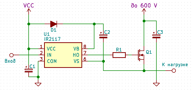
The circuit is not very complicated, and the use of a driver allows the most efficient use of the transistor.
IGBT
Another interesting class of semiconductor devices that can be used as a switch is the insulated gate bipolar transistor (IGBT).
They combine the advantages of both MOS and bipolar transistors: they are controlled by voltage, they have large values of maximum allowable voltages and currents.
You can control the key on the IGBT in the same way as the key on the MOSFET. Due to the fact that IGBTs are used more in power electronics, they are usually used in conjunction with drivers.
For example, according to the datasheet, IR2117 can be used to drive an IGBT.
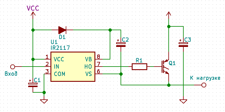
An example of an IGBT is IRG4BC30F.
AC Load Control
All previous schemes were distinguished by the fact that the load, although it was powerful, worked on direct current. The circuits had a clearly defined ground and a power line (or two lines - for the controller and the load).
For AC circuits, other approaches must be used. The most common are the use of thyristors, triacs and relays. We will consider the relay a little later, but for now let's talk about the first two.
Thyristors and triacs
A thyristor is a semiconductor device that can be in two states:
- open - passes current, but only in one direction,
- closed - does not pass current.
Since the thyristor passes current in only one direction, it is not very suitable for turning the load on and off. Half the time for each AC cycle, the instrument is idle. However, a thyristor can be used in a dimmer. There it can be used to control power, cutting off a piece of the required power from the power wave.
A triac is actually a bidirectional thyristor. This means that it allows you to pass not half-waves, but a full wave of the load supply voltage.
There are two ways to open a triac (or thyristor):
- apply (at least briefly) unlocking current to the control electrode;
- submit enough high voltage on its "working" electrodes.
The second method does not suit us, since we will have a constant amplitude supply voltage.
After the triac has opened, it can be closed by reversing the polarity or reducing the current through it to a value less than the so-called holding current. But since the power is organized by alternating current, this will automatically happen at the end of the half-cycle.
When choosing a triac, it is important to consider the magnitude of the holding current ($I_H$). If you take a powerful triac with a large holding current, the current through the load may be too small, and the triac simply will not open.
Triac key
For galvanic isolation of control and power circuits, it is better to use an optocoupler or a special triac driver. For example, MOC3023M or MOC3052.
These optocouplers consist of an infrared LED and a phototriac. This phototriac can be used to control a powerful triac switch.
In the MOC3052, the voltage drop across the LED is 3V and the current is 60mA, so when connecting to a microcontroller, you may need to use an additional transistor switch.
The built-in triac is designed for voltage up to 600 V and current up to 1 A. This is enough to control powerful household appliances through the second power triac.
Consider a circuit for controlling a resistive load (for example, an incandescent lamp).
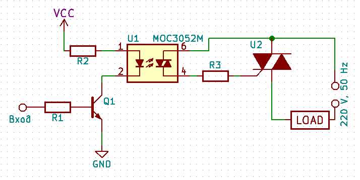
Thus, this optocoupler acts as a triac driver.
There are also drivers with a zero detector - for example, MOC3061. They switch only at the beginning of the period, which reduces interference in the mains.
Resistors R1 and R2 are calculated as usual. The resistance of the resistor R3 is determined based on the peak voltage in the power supply network and the unlocking current of the power triac. If you take too much - the triac will not open, too small - the current will flow in vain. The resistor may need a powerful one.
It would be useful to recall that 220 V in the mains is the value of the effective voltage. The peak voltage is $\sqrt2 \cdot 220 \approx 310\,V$.
Inductive load control
When driving an inductive load, such as a motor, or when there is interference in the mains, the voltage can become large enough for the triac to spontaneously open. To combat this phenomenon, it is necessary to add a snubber to the circuit - this is a smoothing capacitor and a resistor in parallel with the triac.
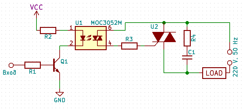
Snubber doesn't improve emissions much, but it's better with it than without it.
The ceramic capacitor must be designed for a voltage greater than the peak voltage in the power supply. Let us remember once again that for 220 V it is 310 V. It is better to take it with a margin.
Typical values: $C_1 = 0(,)01\,uF$, $R_4 = 33\,Ohm$.
There are also triac models that do not require a snubber. For example, BTA06-600C.
Triac examples
Examples of triacs are shown in the table below. Here $I_H$ is the holding current, $\max\ I_(T(RMS))$ is the maximum current, $\max\ V_(DRM)$ is the maximum voltage, $I_(GT)$ is the trigger current.
| Model | $I_H$ | $\max\ I_(T(RMS))$ | $\max\ V_(DRM)$ | $I_(GT)$ |
|---|---|---|---|---|
| BT134-600D | 10 mA | 4 A | 600 V | 5 mA |
| MAC97A8 | 10 mA | 0.6 A | 600 V | 5 mA |
| Z0607 | 5 mA | 0.8 A | 600 V | 5 mA |
| BTA06-600C | 25 mA | 6 A | 600 V | 50 mA |
Relay
Electromagnetic relays
From the point of view of the microcontroller, the relay itself is a powerful load, moreover, inductive. Therefore, to turn on or turn off the relay, you need to use, for example, a transistor switch. The wiring diagram and also the improvement of this circuit was discussed earlier.
Relays impress with their simplicity and efficiency. For example, the HLS8-22F-5VDC relay is controlled by a voltage of 5 V and is capable of switching a load that consumes current up to 15 A.
Solid State Relays
The main advantage of the relay - ease of use - is overshadowed by several disadvantages:
- this is a mechanical device and the contacts can become dirty or even welded to each other,
- slower switching speed
- comparatively large switching currents,
- contacts click.
Some of these shortcomings are eliminated in the so-called solid state relays. These are, in fact, semiconductor devices with galvanic isolation, containing inside a full-fledged powerful key circuit.
Conclusion
Thus, in the arsenal we have enough ways to control the load to solve almost any problem that may arise in front of a radio amateur.
Schematic editor
All diagrams are drawn in KiCAD. Recently, I use it for my projects, it is very convenient, I recommend it. With it, you can not only draw circuits, but also design printed circuit boards.
Here I separately took out such an important practical issue as the connection of inductive sensors with a transistor output, which are ubiquitous in modern industrial equipment. In addition, there are real instructions for the sensors and links to examples.
The principle of activation (operation) of sensors in this case can be any - inductive (approximation), optical (photoelectric), etc.
The first part described possible options sensor outputs. There should be no problems with connecting sensors with contacts (relay output). And with transistors and with connecting to the controller, not everything is so simple.
Below, for example, are the connection diagrams for sensors with a transistor output. The load is usually the input of the controller.
sensor. The load (Load) is constantly connected to the “minus” (0V), the supply of discrete “1” (+V) is switched by a transistor. NO or NC sensor - depends on the control circuit (Main circuit)
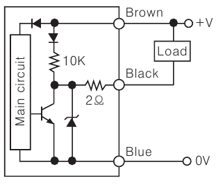
sensor. Load (Load) is constantly connected to the "plus" (+V). Here, the active level (discrete "1") at the output of the sensor is low (0V), while the load is powered through the opened transistor.
I urge everyone not to get confused, the work of these schemes will be described in detail later.
The diagrams below show basically the same thing. The emphasis is on the differences in the circuits of PNP and NPN outputs.
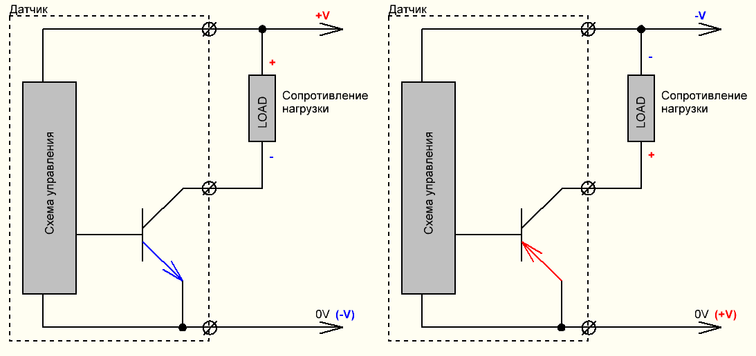
On the left figure - a sensor with an output transistor NPN. A common wire is switched, which in this case- negative wire of the power supply.
Right - the case with a transistor PNP at the exit. This case is the most frequent, since in modern electronics it is customary to make the negative wire of the power source common, and activate the inputs of controllers and other recording devices with a positive potential.
How to test an inductive sensor?
To do this, you need to apply power to it, that is, connect it to the circuit. Then - activate (initiate) it. When activated, the indicator will light up. However, the indication does not guarantee the correct operation of the inductive sensor. You need to connect the load, and measure the voltage on it to be 100% sure.
Replacement of sensors
As I already wrote, there are basically 4 types of sensors with a transistor output, which are divided according to their internal structure and switching circuit:
- PNP NO
- PNP NC
- NPN NO
- NPN NC
All these types of sensors can be replaced with each other, i.e. they are interchangeable.
This is implemented in the following ways:
- Alteration of the initiation device - the design changes mechanically.
- Changing the existing scheme for switching on the sensor.
- Switching the type of sensor output (if there are such switches on the sensor body).
- Program reprogramming - changing the active level of this input, changing the program algorithm.
Below is an example of how you can replace a PNP sensor with an NPN one by changing the wiring diagram:
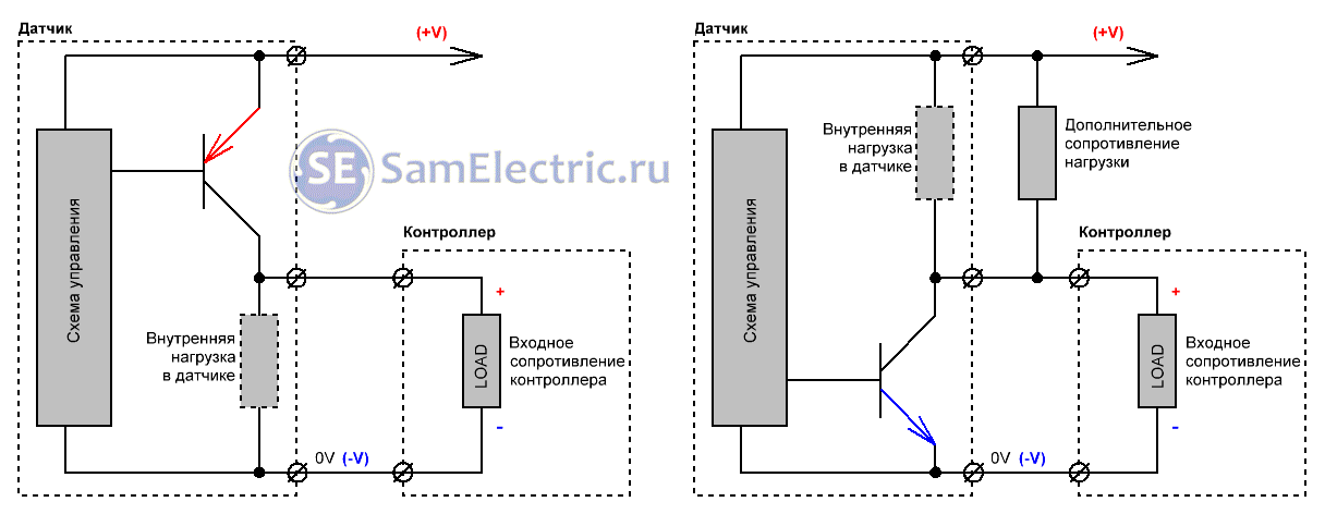
PNP-NPN replacement. On the left is the original diagram, on the right is the modified one.
Understanding the operation of these circuits will help the realization of the fact that the transistor is a key element that can be represented by ordinary relay contacts (examples are below, in the notation).
So the diagram is on the left. Let's assume that the sensor type is NO. Then (regardless of the type of transistor at the output), when the sensor is not active, its output "contacts" are open, and no current flows through them. When the sensor is active, the contacts are closed, with all the ensuing consequences. More precisely, with current flowing through these contacts)). The flowing current creates a voltage drop across the load.
The internal load is shown by the dotted line for a reason. This resistor exists, but its presence does not guarantee stable operation of the sensor, the sensor must be connected to the controller input or other load. The resistance of this input is the main load.
If there is no internal load in the sensor, and the collector "hangs in the air", then this is called an "open collector circuit". This circuit ONLY works with a connected load.
Maybe this will be interesting:
So, in a circuit with a PNP output, when activated, the voltage (+V) through the open transistor enters the controller input, and it is activated. How to achieve the same with the release of NPN?
There are situations when the required sensor is not at hand, and the machine should work “right now”.
We look at the changes in the scheme on the right. First of all, the mode of operation of the output transistor of the sensor is provided. For this, an additional resistor is added to the circuit, its resistance is usually of the order of 5.1 - 10 kOhm. Now, when the sensor is not active, voltage (+V) is supplied to the controller input through an additional resistor, and the controller input is activated. When the sensor is active, there is a discrete “0” at the controller input, since the controller input is shunted by an open NPN transistor, and almost all the current of the additional resistor passes through this transistor.
Yes, not quite what we wanted. In this case, there is a rephasing of the sensor operation. But the sensor works in the mode, and the controller receives information. In most cases, this is sufficient. For example, in the pulse counting mode - a tachometer, or the number of blanks.
How to achieve full functionality? Method 1 - mechanically move or remake a metal plate (activator). Or the light gap, if we are talking about an optical sensor. Method 2 - reprogram the controller input so that discrete "0" is the active state of the controller, and "1" is passive. If you have a laptop at hand, then the second method is both faster and easier.
Proximity sensor symbol
On the circuit diagrams inductive sensors (proximity sensors) are designated differently. But the main thing is that there is a square rotated by 45 ° and two vertical lines in it. As in the diagrams below.

NO NC sensors. Principal schemes.
On the top diagram there is a normally open (NO) contact (conditionally marked PNP transistor). The second circuit is normally closed, and the third circuit is both contacts in one housing.
Color coding of sensor outputs
There is a standard sensor marking system. All manufacturers currently adhere to it.
However, it is useful to make sure that the connection is correct before installation by referring to the connection manual (instructions). In addition, as a rule, the colors of the wires are indicated on the sensor itself, if its size allows.
Here is the marking.
Blue (Blue) - Minus power
Brown (Brown) - Plus
Black (Black) - Exit
White (White) - the second output, or control input, you have to look at the instructions.
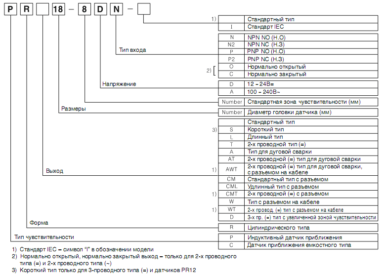
Designation system for inductive sensors
The sensor type is indicated by an alphanumeric code that encodes the main parameters of the sensor. Below is the labeling system for popular Autonics gauges.
Download instructions and manuals for some types of inductive sensors:
/ Inductive proximity sensors. Detailed description parameters, pdf, 135.28 kB, downloaded: 1183 times./Real sensors
It is problematic to buy sensors, the product is specific, and electricians do not sell such in stores. Alternatively, they can be bought in China, on Aliexpress.
Thank you all for your attention, I'm waiting for questions on connecting sensors in the comments!