Volt-ampere characteristics of the diode. Characteristics and principle of operation of rectifier diodes
Rectifier diode is an electronic device designed to convert alternating current into direct current. This is a two-electrode device that has only one-sided (unipolar) electrical conductivity. A rectifier diode made of semiconductor materials and the so-called (when four diodes are connected diagonally in pairs in one housing) replaced the ignitron and the vacuum diode.
The effect of rectifying alternating current and converting it into direct current occurs at the semiconductor-metal, metal-semiconductor junction, or in the so-called electron-hole junction in some crystals (for example, silicon, germanium, selenium, cuprous oxide). Such crystals often serve as the basis of the device.
Semiconductor rectifier diodes are used in radio engineering, electronic and electrical devices. Essentially, rectification is the conversion of alternating current (voltage) into a current of one polarity (pulsating direct). This type of rectification in technology is necessary for opening and closing electrical circuits, switching and detecting electrical signals and pulses, and for many other similar transformations. Such diode characteristics as speed, stability of parameters, capacitance p-n transitions are not obliged to impose any special requirements on themselves.
Such a device has certain electrical parameters and characteristics of diodes:
Forward voltage at a specified current value (taken ;
Reverse current at a given value of reverse voltage and temperature;
Amplitude permissible values for maximum reverse voltage;
Average value of forward current;
Frequency value without mode reduction;
Resistance.
A rectifier diode is often abbreviated to simply a rectifier. As a component of an electrical circuit, it offers high resistance to current flowing in one direction and low resistance to current flowing in the opposite direction. This is what causes
A device such as a rectifier diode has a fairly low operating frequency for industrial use of such a device when converting alternating current to direct current is 50 Hz. The limiting frequency is considered to be no more than 20 kHz.
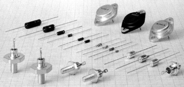
A rectifying diode as an electronic device can be divided into several groups according to the value of the maximum average forward current. These are low-power diodes (up to 0.3 amperes), medium-power diodes (from 0.3 A to 10 A) and heavy-duty (power) rectifier diodes (more than ten amperes).
The main parameters of such an electronic device as a rectifier diode also include the operating range for temperature environment(usually it ranges from -50 to +130 degrees Celsius for the most common type of diode - silicon) and the maximum temperature of the case (very different parameters, depending on the power, purpose and manufacturer).
There are many devices created for the purpose of converting electric current, and rectifying diodes are one of them.
Rectifier diode – converter of alternating current into direct current. It is a type of semiconductor. Wide Application received thanks to the main characteristic - the transfer of electric current strictly in one direction.
Operating principle
The required effect during operation of the device is created p-n features transition. They consist in the fact that a layer is built near the junction of two semiconductors, which is characterized by two points: high resistance and the absence of charge carriers. Further, when this barrier layer is exposed to alternating voltage from the outside, its thickness decreases and subsequently disappears. The current that increases during this is the direct current that passes from the anode to the cathode. If the polarity of the external alternating voltage changes, the blocking layer will be larger and the resistance will inevitably increase.
The current-voltage characteristic of the rectifier diode (volt-ampere characteristic) also gives an idea of the specifics of the rectifier’s operation and is nonlinear. It looks like this: there are two branches - forward and reverse. The first reflects the highest conductivity of the semiconductor when a direct potential difference occurs. The second indicates the value of low conductivity at an inverse potential difference.
The current-voltage characteristics of the rectifier are directly proportional to the temperature, with an increase in which the potential difference decreases. Electric current will not pass through the device in the case of low conductivity, but an avalanche breakdown occurs if the reverse voltage increases to a certain level.
Using an assembly
When operating a semiconductor diode rectifier, only half of the alternating current waves are useful, and more than half of the input voltage is therefore irretrievably lost.
In order to improve the quality of conversion of alternating current to direct current, an assembly of four devices is used - a diode bridge. It differs favorably in that it passes current during each half-cycle. Diode bridges are produced in the form of a kit enclosed in a plastic case.
 Schematic diagram diode bridge
 Physical and technical parameters
The main parameters of rectifier diodes are based on the following values:
- the maximum permissible value of the potential difference when rectifying the current, at which the device will not fail;
- the highest average rectified current;
- the highest reverse voltage value.
The industry produces rectifiers with different physical characteristics. Accordingly, devices have different shapes and installation method. They are divided into three groups:
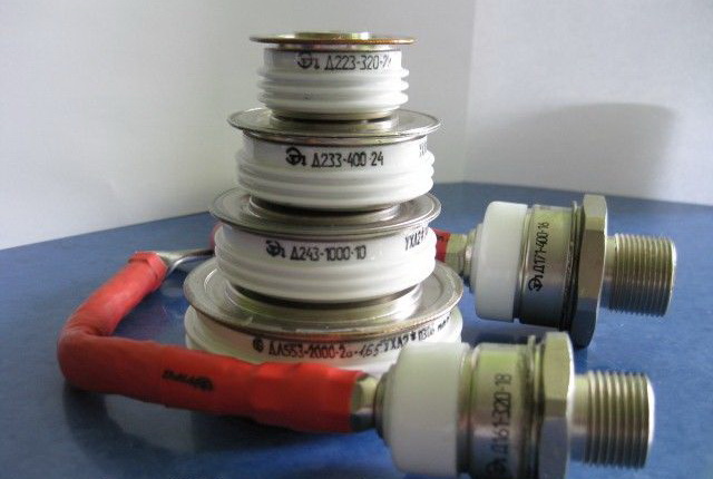
- High power rectifier diodes. They are characterized by a current capacity of up to 400 A and are high-voltage. High-voltage rectifier diodes are produced in two types of packages - pin, where the case is sealed and glass, and tablet, where the case is made of ceramic.
- Medium power rectifier diodes. They have a capacity from 300 mA to 10A.
- Low power rectifier diodes. The maximum permissible current value is up to 300 mA.
Selection of rectifier diodes
When purchasing a device, you must be guided by the following parameters:
- values of the current-voltage characteristic of the maximum reverse and peak current;
- maximum permissible reverse and forward voltage;
- average rectified current strength;
- device material and type of installation.
Depending on the physical characteristics The corresponding designation is applied to the device body. A catalog with markings of rectifier diodes is presented in a specialized reference book. You need to know that the labeling of imported analogues differs from domestic ones.
It is also worth paying attention to the fact that rectifier circuits differ in the number of phases:
- Single-phase. Widely used for household electrical appliances. There are diodes for automobiles and for electric arc welding.
- Multiphase. Indispensable for industrial equipment, public and special transport.
Schottky diode
A special position is occupied by the Schottky diode. It was invented in connection with the growing needs in the developing radio electronics industry. Its main difference from other diodes is that its design includes a metal-semiconductor like p-n alternative transition. Accordingly, the Schottky diode has its own, unique properties, which silicon rectifier diodes cannot boast of. Some of them:
- operational renewability of the charge due to its low value;
- minimum voltage drop across the junction when connected directly;
- The leakage current is significant.
When making a Schottky diode, materials such as silicon and gallium arsenide are used, but germanium is also sometimes used. The properties of the materials are slightly different, but in any case, the maximum permissible reverse voltage for a Schottky rectifier is no more than 1200 V.
In contrast to all the advantages, the design of this type also has disadvantages. For example, in a bridge assembly, the device categorically does not perceive excess reverse current. Violation of the condition leads to breakdown of the rectifier. Also, a small voltage drop occurs at a low voltage of about 60-70 V. If the value exceeds this indicator, then the device turns into an ordinary rectifier.
It is worth noting that the advantages of a powerful Schottky rectifier diode significantly exceed the disadvantages.
Zener diode
To stabilize the voltage, a special device is used that can operate in breakdown mode - a zener diode, the foreign name of which is “Zener diode”. The device performs its function by operating in breakdown mode at a reverse bias voltage. The current increases at the moment of breakdown; at the same time, the differential value drops to a minimum, as a result of which the voltage is stable and covers a fairly serious range of reverse currents.
Practical use of rectifier diode
Due to the unstoppable development of scientific and technological progress, the use of rectifiers has affected all spheres of human activity. Power rectifier diodes are used in the following components and mechanisms:
- in power supplies for main engines of vehicles (land, air and water), industrial machines and equipment, drilling rigs;
- complete with diode bridge for welding machines;
- in rectifying installations for galvanic baths used for producing non-ferrous metals or applying a protective coating to a part or product;
- in rectifier installations for water and air purification, filters of various kinds;
- for transmitting electricity over long distances via high-voltage power lines.
IN Everyday life rectifiers are used in various transistor circuits. Low-power devices are mainly used, both in the form of a half-wave rectifier and in the form of a diode bridge. For example, the diodes of the generator rectifier unit are well known to car enthusiasts.
TOPIC 3. SEMICONDUCTOR DIODES
A semiconductor diode is an electrical converting semiconductor device with one electrical junction and two terminals, which uses the properties pn junction.
Semiconductor diodes are classified:
1) by purpose: rectifier, high-frequency and ultra-high-frequency (HF and microwave diodes), pulse, semiconductor zener diodes (reference diodes), tunnel diodes, reverse diodes, varicaps, etc.;
2) according to design and technological features: planar and point;
3) by type of source material: germanium, silicon, arsenide-gallium, etc.
Figure 3.1 – Design of point diodes
A point diode uses a germanium or silicon plate with n-type electrical conductivity (Fig. 3.1), 0.1...0.6 mm thick and 0.5...1.5 mm2 in area; A sharpened wire (needle) with an impurity deposited on it comes into contact with the plate. In this case, impurities diffuse from the needle into the main semiconductor, which create an area with a different type of electrical conductivity. Thus, a miniature hemispherical pn junction is formed near the needle.
To make germanium point diodes, a tungsten wire coated with indium is welded to a germanium plate. Indium is an acceptor for germanium. The resulting region of p-type germanium is emitter.
Silicon point diodes are made using n-type silicon and a wire coated with aluminum, which serves as an acceptor for the silicon.
In planar diodes, the pn junction is formed by two semiconductors with different types of electrical conductivity, and the junction area is various types diodes range from hundredths of a square millimeter to several tens of square centimeters (power diodes).
Planar diodes are manufactured by fusion (fusing) or diffusion methods (Fig. 3.2).
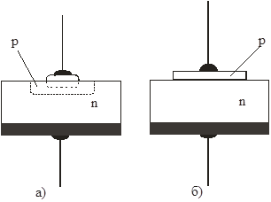
Figure 3.2 – Design of planar diodes manufactured by the alloy (a) and diffusion method (b)
A drop of indium is fused into a plate of n-type germanium at a temperature of about 500°C (Fig. 3.2, a), which, fused with germanium, forms a layer of p-type germanium. The region with p-type electrical conductivity has a higher impurity concentration than the main plate and is therefore an emitter. Lead wires, usually made of nickel, are soldered to the main germanium plate and to the indium plate. If p-type germanium is taken as the starting material, then antimony is smelted into it and then an n-type emitter region is obtained.
The diffusion method of manufacturing a p-n junction is based on the fact that impurity atoms diffuse into the main semiconductor (Fig. 3.2, b). To create a p-layer, the diffusion of an acceptor element (boron or aluminum for silicon, indium for germanium) through the surface of the source material is used.
3.1 Rectifier diodes
A rectifying semiconductor diode is a semiconductor diode designed to convert alternating current into direct current.
Rectifier diodes are made on the basis of a pn junction and have two regions, one of them is lower resistance (contains a higher impurity concentration), and is called the emitter. The other area, the base, is more highly resistant (contains a lower concentration of impurities).
The operation of rectifier diodes is based on the property of one-way conductivity of the p-n junction, which lies in the fact that the latter conducts current well (has low resistance) when connected directly and practically does not conduct current (has a very high resistance) when connected in reverse.
As is known, the forward current of the diode is created by the main ones, and the reverse current is created by non-primary charge carriers. The concentration of majority charge carriers is several orders of magnitude higher than the concentration of non-majority carriers, which determines the valve properties of the diode.
The main parameters of rectifying semiconductor diodes are:
· forward current of the diode Ipr, which is normalized at a certain forward voltage (usually Upr = 1...2V);
· maximum permissible forward current Ipr max diode;
· the maximum permissible reverse voltage of the diode Urev max, at which the diode can still operate normally for a long time;
· constant reverse current Irev flowing through the diode at a reverse voltage equal to Urev max;
· average rectified current Ivp.sr, which can pass through the diode for a long time at an acceptable temperature of its heating;
· maximum permissible power Pmax dissipated by the diode, at which the specified reliability of the diode is ensured.
According to the maximum permissible value of the average rectified current, diodes are divided into low-power (Ivp.av £ 0.3A), medium-power (0.3A
To maintain the performance of a germanium diode, its temperature should not exceed +85°C. Silicon diodes can operate at temperatures up to +150°C.
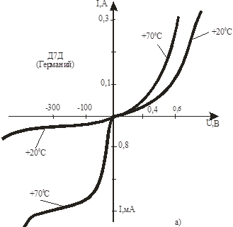

Figure 3.3 – Change in the volt-ampere characteristics of a semiconductor diode depending on temperature: a – for a germanium diode; b – for a silicon diode
The voltage drop when passing direct current for germanium diodes is DUpr = 0.3...0.6V, for silicon diodes - DUpr = 0.8...1.2V. Large voltage drops when direct current passes through silicon diodes compared to direct voltage drops on germanium diodes are associated with a higher potential barrier height of p-n junctions formed in silicon.
With increasing temperature, the forward voltage drop decreases, which is associated with a decrease in the height of the potential barrier.
When a reverse voltage is applied to a semiconductor diode, a slight reverse current arises in it, due to the movement of minority charge carriers through the pn junction.
As the temperature of the pn junction increases, the number of minority charge carriers increases due to the transition of some electrons from the valence band to the conduction band and the formation of electron-hole charge carrier pairs. Therefore, the reverse current of the diode increases.
When a reverse voltage of several hundred volts is applied to the diode, the external electric field in the blocking layer becomes so strong that it can pull electrons from the valence band into the conduction band (Zener effect). In this case, the reverse current increases sharply, which causes heating of the diode, a further increase in the current and, finally, thermal breakdown (destruction) of the p-n junction. Most diodes can operate reliably at reverse voltages not exceeding (0.7...0.8) Uprob.
The permissible reverse voltage of germanium diodes reaches - 100...400V, and for silicon diodes - 1000...1500V.
In a number of powerful converter installations, the requirements for the average value of the forward current and reverse voltage exceed the nominal value of the parameters of existing diodes. In these cases, the problem is solved by parallel or series connection of diodes.
Parallel connection of diodes is used when it is necessary to obtain a forward current greater than the limiting current of one diode. But if diodes of the same type are simply connected in parallel, then, due to the mismatch of the direct branches of the current-voltage characteristic, they will be differently loaded and, in some, the forward current will be greater than the limiting one.
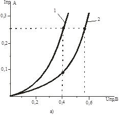
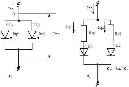
Figure 3.4 – Parallel connection of rectifier diodes
To equalize the currents, diodes with a small difference in the direct branches of the current-voltage characteristic are used (they are selected) or equalizing resistors with a resistance of units of Ohms are connected in series with the diodes. Sometimes additional resistors are included (Fig. 3.4, c) with a resistance several times greater than the direct resistance of the diodes, so that the current in each diode is determined mainly by the resistance Rd, i.e. Rd>>rpr vd. The value of Rd is hundreds of ohms.
Series connection of diodes is used to increase the total permissible reverse voltage. When exposed to reverse voltage, the same reverse current Irev flows through diodes connected in series. however, due to the difference in the reverse branches of the current-voltage characteristic, the total voltage will be distributed unevenly across the diodes. A diode whose reverse branch of the current-voltage characteristic is higher will have a greater voltage applied to it. It may be higher than the limit, which will lead to breakdown of the diodes.
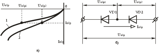
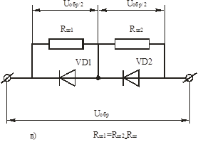
Figure 3.5 – Series connection of rectifier diodes
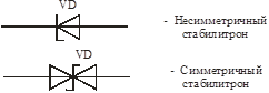
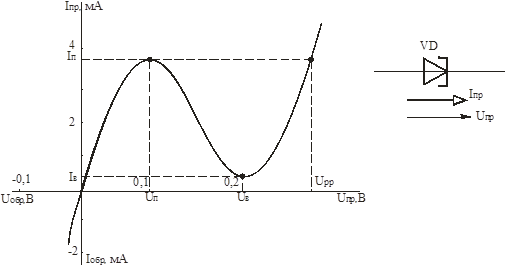
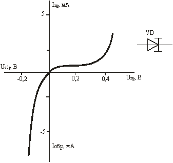
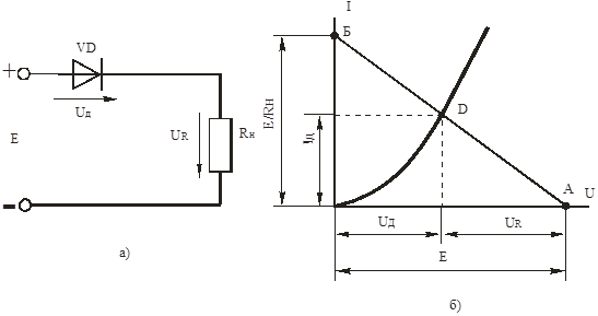
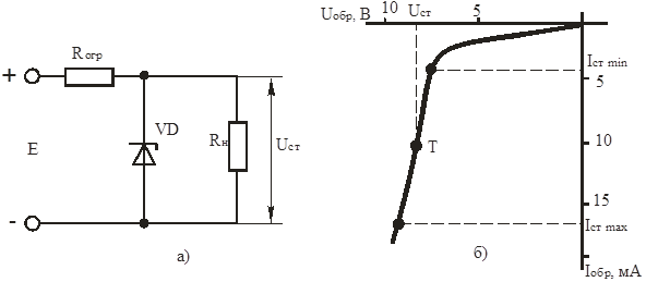
To ensure that the reverse voltage is distributed evenly between the diodes regardless of their reverse resistance, diodes are shunted with resistors. The resistances Rsh of the resistors must be the same and significantly less than the smallest reverse resistance of the diodes Rsh< 3.2 Zener diodes A semiconductor zener diode is a semiconductor diode, the voltage on which in the region of electrical breakdown weakly depends on the current and which is used to stabilize the voltage. Semiconductor zener diodes use the property of a slight change in the reverse voltage at the p-n junction during an electrical (avalanche or tunnel) breakdown. This is due to the fact that a small increase in the voltage at the pn junction in the electrical breakdown mode causes a more intense generation of charge carriers and a significant increase in the reverse current. Low-voltage zener diodes are made on the basis of heavily alloyed (low-resistance) material. In this case, a narrow planar junction is formed, in which a tunneling electrical breakdown occurs at relatively low reverse voltages (less than 6V). High-voltage zener diodes are made on the basis of lightly alloyed (high-resistance) material. Therefore, their principle of operation is associated with avalanche electrical breakdown. Main parameters of zener diodes: · stabilization voltage Ust (Ust = 1…1000V); · minimum Ist mіn and maximum Ist max stabilization currents (Ist mіn" 1.0...10 mA, Ist max "0.05...2.0A); · maximum permissible power dissipation Рmax; · differential resistance in the stabilization section rd = DUst/DIst, (rd" 0.5...200 Ohm); temperature coefficient of voltage in the stabilization section: TKU of a zener diode shows by what percentage the stabilizing voltage will change when the temperature of the semiconductor changes by 1°C (TKU= −0.5…+0.2%/°С). Figure 3.6 – Volt-ampere characteristic of the zener diode and its symbolic graphic designation Zener diodes are used to stabilize the voltages of power supplies, as well as to fix voltage levels in various circuits. Stabilization of low-voltage voltage within 0.3...1V can be achieved by using the direct branch of the I-V characteristic of silicon diodes. A diode in which the direct branch of the current-voltage characteristic is used to stabilize the voltage is called a stabistor. There are also double-sided (symmetrical) zener diodes that have a symmetrical current-voltage characteristic relative to the origin. Zener diodes can be connected in series, with the resulting stabilizing voltage equal to the sum of the zener diode voltages: Ust = Ust1 + Ust2 +… Parallel connection of zener diodes is unacceptable, because due to the scatter of characteristics and parameters of all parallel-connected zener diodes, current will arise only in one, which has the lowest stabilizing voltage Ust, which will cause overheating of the zener diode. 3.3 Tunnel and reverse diodes A tunnel diode is a semiconductor diode based on a degenerate semiconductor, in which the tunnel effect leads to the appearance of a negative differential resistance section on the current-voltage characteristic at forward voltage. The tunnel diode is made of germanium or gallium arsenide with a very high concentration of impurities, i.e. with very low resistivity. Such semiconductors with low resistance are called degenerate. This makes it possible to obtain a very narrow pn junction. In such transitions, conditions arise for relatively free tunneling of electrons through a potential barrier (tunnel effect). The tunnel effect leads to the appearance of a section with negative differential resistance on the direct branch of the diode’s current-voltage characteristic. The tunnel effect is that at a sufficiently low height of the potential barrier, electrons can penetrate through the barrier without changing their energy. Main parameters of tunnel diodes: · peak current Iп – forward current at the maximum point of the current-voltage characteristic; · valley current Iв – forward current at the minimum point of the current-voltage characteristic; · ratio of tunnel diode currents Iп/Iв; · peak voltage Uп – forward voltage corresponding to the peak current; · valley voltage Uв – forward voltage corresponding to the valley current; · solution voltage Uрр. Tunnel diodes are used to generate and amplify electromagnetic oscillations, as well as in high-speed switching and pulse circuits. Figure 3.7 – Current-voltage characteristic of a tunnel diode A reverse diode is a diode based on a semiconductor with a critical concentration of impurities, in which the conductivity at reverse voltage due to the tunneling effect is significantly greater than at forward voltage. The principle of operation of a reverse diode is based on the use of the tunnel effect. But in reverse diodes the concentration of impurities is lower than in conventional tunnel diodes. Therefore, the contact potential difference for reversed diodes is smaller, and the thickness of the pn junction is greater. This leads to the fact that under the influence of direct voltage, a direct tunnel current is not created. The forward current in reversed diodes is created by the injection of non-majority charge carriers through the p-n junction, i.e. direct current is diffusion. When the voltage is reversed, a significant tunneling current flows through the junction, created by the movement of electrons through the potential barrier from the p-region to the n-region. The working section of the current-voltage characteristic of a reversed diode is the reverse branch. Thus, reversed diodes have a rectifying effect, but their passing (conducting) direction corresponds to reverse connection, and the blocking (non-conducting) direction corresponds to direct connection. Figure 3.8 – Volt-ampere characteristic of a reversed diode Reversed diodes are used in pulsed devices, and also as signal converters (mixers and detectors) in radio engineering devices. 3.4 Varicaps A varicap is a semiconductor diode that uses the dependence of capacitance on the magnitude of the reverse voltage and is intended for use as an element with electrically controlled capacitance. The semiconductor material for the manufacture of varicaps is silicon. Basic parameters of varicaps: · nominal capacitance Sv – capacitance at a given reverse voltage (Sv = 10...500 pF); · capacity overlap coefficient; (Ks = 5...20) – the ratio of the varicap capacitances at two given values of reverse voltages. Varicaps are widely used in various circuits for automatic frequency adjustment and in parametric amplifiers. Figure 3.9 – Capacitance-voltage characteristic of a varicap 3.5 Calculation of electrical circuits with semiconductor diodes. In practical circuits, some load, for example a resistor, is connected to the diode circuit (Fig. 3.10, a). Direct current flows when the anode has a positive potential relative to the cathode. The mode of the diode with a load is called the operating mode. If the diode had linear resistance, then calculating the current in such a circuit would not be difficult, since the total resistance of the circuit is equal to the sum of the diode's resistance to direct current Ro and the resistance of the load resistor Rн. But the diode has a nonlinear resistance, and its Ro value changes as the current changes. Therefore, the current calculation is done graphically. The task is as follows: the values of E, Rn and the characteristics of the diode are known; it is required to determine the current in the circuit I and the voltage on the diode Ud. Figure 3.10 The diode characteristic should be considered as a graph of some equation connecting the quantities I and U. And for resistance Rн, a similar equation is Ohm’s law: So, there are two equations with two unknowns I and U, and one of the equations is given graphically. To solve such a system of equations, you need to construct a graph of the second equation and find the coordinates of the point of intersection of the two graphs. The equation for resistance Rн is an equation of the first degree with respect to I and U. Its graph is a straight line called the load line. It is constructed using two points on the coordinate axes. For I= 0, from equation (3.1) we obtain: E − U= 0 or U= E, which corresponds to point A in Fig. 3.10, b. And if U= 0, then I= E/Rн. we plot this current on the ordinate axis (point B). We draw a straight line through points A and B, which is the load line. The coordinates of point D give the solution to the problem. It should be noted that a graphical calculation of the diode operating mode can be omitted if Rн >> Ro. In this case, it is permissible to neglect the resistance of the diode and determine the current approximately: I»E/Rн. Considered calculation method DC voltage can be applied to amplitude or instantaneous values if the source provides alternating voltage. Since semiconductor diodes conduct current well in the forward direction and poorly in the reverse direction, most semiconductor diodes are used to rectify alternating current. The simplest circuit for rectifying alternating current is shown in Fig. 3.11. It is connected in series with a source of alternating emf - e, a diode VD and a load resistor Rн. This circuit is called half-wave. The simplest rectifier works as follows. During one half-cycle, the voltage for the diode is direct and a current passes, creating a voltage drop UR across the resistor Rн. During the next half-cycle, the voltage is reversed, there is practically no current and UR = 0. Thus, a pulsating current passes through the diode and load resistor in the form of pulses lasting half a cycle. This current is called rectified current. It creates a rectified voltage across the resistor Rн. Graphs in Fig. 3.11, b illustrate the processes in the rectifier. Figure 3.11 The amplitude of the positive half-waves on the diode is very small. This is explained by the fact that when direct current passes, most of the source voltage drops across the load resistor Rн, the resistance of which significantly exceeds the resistance of the diode. In this case For conventional semiconductor diodes, the forward voltage is no more than 1...2V. For example, let the source have an effective voltage E = 200V and With a negative half-wave of the supplied voltage, there is practically no current and the voltage drop across the resistor Rн is zero. The entire source voltage is applied to the diode and is the reverse voltage for it. Thus, maximum value the reverse voltage is equal to the amplitude of the source emf. The simplest diagram of using a zener diode is shown in Fig. 3.12, a. The load (consumer) is connected in parallel with the zener diode. Therefore, in stabilization mode, when the voltage on the zener diode is almost constant, the same voltage will be on the load. Usually Rogr is calculated for the midpoint T of the zener diode characteristics. Let's consider the case when E = const, and Rн varies from Rн min to Rн max.. The value of Rolim can be found using the following formula: where Iav = 0.5(Ist min+Ist max) – average zener diode current; Iн = Ust/Rн – load current (at Rн = const); In.av = 0.5(In min+In max), (with Rn = var), and Figure 3.12 The operation of the circuit in this mode can be explained as follows. Since Rogr is constant and the voltage drop across it, equal to (E − Ust), is also constant, then the current in Rogr, equal to (Ist + In.sr), must be constant. But the latter is only possible if the zener diode current I and the load current Iн change to the same extent, but in opposite directions. For example, if In increases, then the current I decreases by the same amount, and their sum remains unchanged. Let's consider the principle of operation of a zener diode using the example of a circuit consisting of a series-connected source of variable EMF - e, a zener diode VD and a resistor R (Fig. 3.13, a). During the positive half-cycle, a reverse voltage is applied to the zener diode, and up to the breakdown voltage of the zener diode, all voltage is applied to the zener diode, since the current in the circuit is zero. After electrical breakdown of the zener diode, the voltage on the zener diode VD remains unchanged and the entire remaining voltage of the EMF source will be applied to resistor R. During the negative half-cycle, the zener diode is switched on in the conducting direction, the voltage drop across it is about 1V, and the remaining voltage of the EMF source is applied to resistor R. The properties of a diode are determined by its current-voltage characteristic (volt-ampere characteristic), which is shown in Fig. 2.7. It can be approximately described by the equation I=I 0 (e U / m j t – 1), (2.1) Where I 0 – saturation current of the reverse-biased junction (reverse thermal current); U– voltage at p-n– transition; j t = kT/q– thermal potential equal to the contact potential difference j k at the boundary p-n transition in the absence of external voltage; k=1.38×10 -23 J/K – Boltzmann’s constant; T– absolute temperature; q=1.6×10 -19 coulomb – electron charge; m– correction factor taking into account deviations from the theory. At a temperature T=300K, j t =0.026 V. There are two branches on the current-voltage characteristic: direct branch, which is in the first square and reverse branch in the third square. Equation (2.1) well describes the characteristics of a real diode in the forward direction and for small currents. In accordance with (2.1), the diode resistance is nonlinear. In the case of linear resistance, the current-voltage characteristic would be a straight line. On the straight branch of the real current-voltage characteristic there is a sharp bend, which is characterized by switching voltage. For germanium diodes the turn-on voltage is approximately 0.3 V, for silicon diodes it is approximately 0.6 V. The value of the reverse current on the return branch is approximately constant over a wide voltage range. When a certain reverse voltage value, called breakdown voltage, is exceeded U samples, an avalanche-like process of reverse current growth begins, corresponding to electrical breakdown p - n– transition. If the current is not limited at this moment, the electrical breakdown will turn into a thermal breakdown. Thermal breakdown is caused by an increase in the number of carriers in p-n- transition. In this case, the power released in the diode U arr. I the return does not have time to be diverted from the junction, its temperature rises, the reverse current grows and, consequently, the power continues to grow. Thermal breakdown is irreversible, because destroys p–n– transition. For a diode there are several stipulations main parameters: Rated forward current; Maximum reverse voltage; Forward voltage drop; Constant reverse current; Maximum forward current (the operating mode is specified for it, for example, conduction time). Silicon diodes predominate, since they have a higher maximum operating temperature (150 o C versus 75 o C for germanium diodes), allow a higher forward current density (60 ¸ 80 A/cm 2 compared to 20 ¸ 30 A/cm 2), and have lower reverse currents (about an order of magnitude) and higher permissible reverse voltages (1500-2800 V compared to 600-800 V). However, silicon diodes have a higher forward voltage drop, which. for germanium diodes U pr =0.3¸0.4V, and for silicon diodes U pr =0.6¸1.2 V. The performance of a diode is determined by the power released on it P=UI. U And I refer to a certain point of the current-voltage characteristic. Power determines heat. The working section of the diode on the current-voltage characteristic Fig. 2.7 is marked with a thick line. If the diode starts to operate in non-working areas of the current-voltage characteristic, it fails because the power exceeds the permissible, the heating exceeds the permissible and the diode is destroyed. When considering the operating modes of circuits with diodes, they are represented as idealized devices that are ideal conductors in the forward direction and ideal insulators in the reverse direction. The idealized current-voltage characteristic is shown in Fig. 2.8, and the dependence of the current-voltage characteristic on temperature is shown in Fig. 2.9. Types of diodes The following types of diodes are distinguished by purpose: – rectifying; – pulsed; – high frequency; – Zener diodes and stabilizers. Diodes are also distinguished by power and frequency properties. Rectifier diodes. Designed to operate at frequency voltages up to several kHz and at slow edges of the supply voltage. Not intended for rectangular supply voltage. For rectifier diodes, two main parameters are specified: 1. Direct rated current (average value). Diodes are available for currents of 10 mA–1000 A. The reverse voltage ranges from 10 V to several kV. For high-power diodes (current > 10 A), the reverse voltage is determined by the class of the diode. The diode class is 100V multiplied by the class number. Class number from 1 to 20. For example: D50-12, here 50 is the direct rated current in A; 12th grade. Class is a parameter used for power diodes and characterizes the reverse voltage. For powerful diodes, the rated forward current is permissible only when the diode is installed on a radiator and with forced cooling at an air speed of 12 m/s. Without forced air cooling (there is only a radiator), the permissible current is about 30% of the rated one. The following designations are common for modern diodes: D XXXY or CD XXXY, where CD is a silicon diode, XXX- numbers, Y- letter. The first number indicates the type of diode (rectifier - 1, 2). The letter defines the reverse voltage. Secondary parameters: 1.Maximum reverse current I arr.max (from tens of nA to tens of mA). 2.Forward voltage drop U pr (0.3¸1.2V). 3. The maximum operating frequency up to which the specified currents, voltages and power are provided. 4. Time to restore the blocking properties of the diode. The diode does not conduct (or turn off) when reverse voltage is applied. Blocking is a transition from a conducting state to a non-conducting state. When a square wave reverse voltage is applied, the diode behaves as shown in Fig. 2.10. Interval I is the time of carrier resorption, interval II is the reverse current surge. It is associated with the presence of a barrier capacitance of the diode. Interval t c – recovery time, i.e. the time of transition from the conducting state until the reverse current is established on the current-voltage characteristic. Due to the imperfection of the diode, the maximum frequency of its operation is limited. At very high frequencies, the diode ceases to perform its functions. High frequency diodes. The same parameters (main and secondary) are specified for them, but they can operate at high frequencies and have a short recovery time (compared to rectifiers). For them, a graph of forward current is given as a function of frequency. The graph is shown in Fig. 2.11. Pulse diodes. The same basic parameters are specified as for the diodes discussed above, and an important secondary parameter is also given - the pulse current for a specified time. Zener diodes and stabilizers. The working part of the current-voltage characteristic of zener diodes is the reverse branch. The forward branch is the same as diodes, it can also be used. The current-voltage characteristic of the zener diode is shown in Fig. 2.12. For zener diodes, two main parameters are indicated: U st – stabilization voltage of the zener diode; Ist.n – rated current of the zener diode. U st =3.3¸170V. For U st indicates the spread in percentage or in volts, as well as the change U st when the temperature changes. For low-power zener diodes I st.min =1¸3 m A, I s t. max =30 m A. I st.n for powerful zener diodes is several hundred m A. Stabilizers are zener diodes that use the direct branch of the current-voltage characteristic, i.e. This is a diode with a large voltage drop that is constant as the current changes. The current-voltage characteristic of the stabistor is shown in Fig. 2.13. Such a current-voltage characteristic is created technologically. Zener diodes and stabilizers can be connected in series, but not in parallel. They are used in stabilizers and voltage limiters. 1. What is the potential barrier of a semiconductor diode and how is it formed? 2. Briefly describe the connection circuits of a semiconductor diode. 3. Describe the real and ideal volt-ampere characteristics of a semiconductor diode. 4. List the main parameters of a semiconductor diode. 5. Describe the main types of diodes. 6. List the minor parameters of a semiconductor diode. 7. How is a semiconductor diode marked? Rectifier diodes
are used in control circuits, switching circuits, limiting and decoupling circuits, in power supplies for converting (rectifying) alternating voltage into direct voltage, in voltage multiplying circuits and direct voltage converters, where high demands are not placed on the frequency and time parameters of signals. Depending on the value of the maximum rectified current, there are low power rectifier diodes(\(I_(pr max) \le (0.3 A)\)), medium power(\((0.3 A)< I_{пр max} \le {10 А}\)) и high power(\(I_(pr max) > (10 A)\)). Low-power diodes can dissipate the heat generated on them by their housing; medium and high-power diodes must be located on special heat sinks, which is provided, among other things. and the corresponding design of their bodies. Typically, the permissible current density passing through the \(p\)-\(n\) junction does not exceed 2 A/mm2, therefore, to obtain the above values of the average rectified current in rectifier diodes, planar \(p\)-\ (n\)-transitions. Such junctions have a significant capacitance, which limits the maximum permissible operating frequency (\(f_р\)) of rectifier diodes. The rectifying properties of diodes are better, the lower the reverse current at a given reverse voltage and the lower the voltage drop at a given forward current. The values of the forward and reverse currents differ by several orders of magnitude, and the forward voltage drop does not exceed a few volts compared to the reverse voltage, which can be hundreds or more volts. Therefore, diodes have one-way conductivity, which allows them to be used as rectifier elements. The current-voltage characteristics (CV) of germanium and silicon diodes are different. In Fig. For comparison, Figure 2.3-1 shows typical current-voltage characteristics for germanium and silicon rectifier diodes at different ambient temperatures. Rice. 2.3-1. Current-voltage characteristics of rectifier diodes at different ambient temperatures
From the given current-voltage characteristics it is clear that the reverse current of silicon diodes is significantly less than the reverse current of germanium diodes. In addition, the reverse branch of the current-voltage characteristic of silicon diodes does not have a clearly defined saturation region, which is due to the generation of charge carriers in the \(p\)-\(n\) junction and leakage currents along the surface of the crystal. When a reverse voltage is applied that exceeds a certain threshold level, a sharp increase in the reverse current occurs, which can lead to breakdown of the \(p\)-\(n\) junction. In germanium diodes, due to the large reverse current, the breakdown is thermal in nature. Silicon diodes have a low probability of thermal breakdown; electrical breakdown predominates in them. The breakdown of silicon diodes has an avalanche nature, therefore, unlike germanium diodes, the breakdown voltage increases with increasing temperature. The permissible reverse voltage of silicon diodes (up to 1600 V) significantly exceeds that of germanium diodes. Reverse currents are highly dependent on the junction temperature. The figure shows that with increasing temperature the reverse current increases. For an approximate estimate, we can assume that with an increase in temperature by 10 °C, the reverse current of germanium diodes increases by 2 times, and that of silicon diodes by 2.5 times. The upper limit of the operating temperature range for germanium diodes is 75...80 °C, and for silicon diodes - 125 °C. A significant disadvantage of germanium diodes is their high sensitivity to short-term pulse overloads. Due to the lower reverse current of the silicon diode, its forward current, equal to the current of the germanium diode, is achieved at a higher forward voltage. Therefore, the power dissipated at the same currents is less in germanium diodes than in silicon diodes. Forward voltage at low forward currents, when the voltage drop across the junction predominates, decreases with increasing temperature. At high currents, when the voltage drop across the resistance of the neutral regions of the semiconductor predominates, the dependence of the forward voltage on temperature becomes positive. The point at which there is no dependence of forward voltage on temperature (i.e. this dependence changes sign) is called inversion point. For most low- and medium-power diodes, the permissible forward current, as a rule, does not exceed the inversion point, and for high-power diodes, the permissible current can be higher than this point.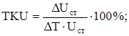

 (3.1)
(3.1)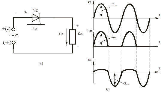
![]() . If Up max = 2V, then URmax = 278V.
. If Up max = 2V, then URmax = 278V.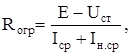 (3.3)
(3.3)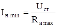 And
And 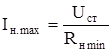 .
.

Rice. 2.7

![]()
Rice. 2.8 Rice. 2.9

Rice. 2.10

Rice. 2.11

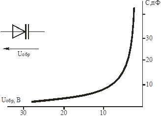
Rice. 2.12 Rice. 2.13