Typical connection diagram for uc3842. Blog › Adjustable power supply based on UC3843 from ATX.
UC3845
PRINCIPLE OF OPERATION
Frankly speaking, it was not possible to defeat the UC3845 the first time - self-confidence played a cruel joke. However, wise with experience, I decided to finally figure it out - the chip is not that big - only 8 legs. I would like to express special gratitude to my subscribers, who did not stand aside and gave some explanations; they even sent a rather detailed article by email and a piece of the model in Microcap. THANK YOU VERY MUCH .
Using the links and materials sent, I sat for an evening or two and, in general, all the puzzles fit together, although some cells turned out to be empty. But first things first...
It was not possible to assemble an analogue of the UC3845 using logic elements in Microcap 8 and 9 - the logic elements are strictly connected to a five-volt power supply, and these simulators have chronic difficulties with self-oscillation. Microcap 11 showed the same results:
There was only one option left - Multisim. Version 12 was even found with a localization. I haven't used Multisim for a VERY long time, so I had to tinker. The first thing that pleased me was that Multisim has a separate library for five-volt logic and a separate library for fifteen-volt logic. In general, with grief in half, it turned out to be a more or less workable option, showing signs of life, but it didn’t want to work exactly the way a real microcircuit behaves, no matter how much I tried to persuade it. Firstly, the models do not measure the level relative to real zero, so an additional source of negative bias voltage would have to be introduced. But in this case they would have to explain in some detail what it is and why, but I wanted to be as close as possible to the real microcircuit.
Having rummaged through the Internet, I found a ready-made scheme, but for Multisim 13. I downloaded option 14, opened the model and it even worked, but the joy did not last long. Despite the presence in the libraries themselves of both the twelfth and fourteenth Multisim of the UC3845 microcircuit itself and its analogues, it quickly became clear that the model of the microcircuit does not allow working out ALL options for switching on this microcircuit. In particular, limiting the current and adjusting the output voltage work quite reliably (though it often falls out of the simulation), but the microcircuit refused to accept the use of applying a ground error to the output of the amplifier.
In general, although the cart moved, it did not travel far. There was only one option left - printing out the datasheet on the UC3845 and a board with wiring. In order not to get carried away with simulating the load and simulating current limiting, I decided to build a microbooster and use it to check what actually happens to the microcircuit under one or another variant of inclusion and use.
First, a little explanation:
The UC3845 microcircuit really deserves the attention of designers of power supplies of various powers and purposes; it has a number of almost analogues. Almost because when replacing a chip on a board, you don’t need to change anything else, but changes in ambient temperature can cause problems. And some sub-options cannot be used as a direct replacement at all.
| VOLTAGE TURN ON - 16 V, OFF - 10 V |
VOLTAGE ON - 8.4 V, OFF - 7.6 V |
WORKING TEMPERATURE | COF FILLING |
| UC1842 | UC1843 | -55°С... +125°С | up to 100% |
| UC2842 | UC2843 | -40°С... +85°С | |
| UC3842 | UC3843 | 0°С... +70°С | |
| UC1844 | UC1845 | -55°С... +125°С | up to 50% |
| UC2844 | UC2845 | -40°С... +85°С | |
| UC3844 | UC3845 | 0°С... +70°С | |
Based on the table above, it is clear that the UC3845 is far from the best version of this microcircuit, since its lower temperature limit is limited to zero degrees. The reason is quite simple - not everyone stores a welding machine in a heated room, and a situation is possible when you need to weld something in the off-season, but the welder either does not turn on or simply explodes. no, not to shreds, even pieces of power transistors are unlikely to fly out, but there will be no welding in any case, and the welder also needs repairs. Having skimmed through Ali, I came to the conclusion that the problem is completely solvable. Of course, UC3845 is more popular and there are more of them on sale, but UC2845 is also on sale:
UC2845 is of course somewhat more expensive, but in any case it is cheaper than ONE power transistor, so I personally ordered a dozen UC2845 despite the fact that there are still 8 pieces of UC3845 in stock. Well, as you wish.
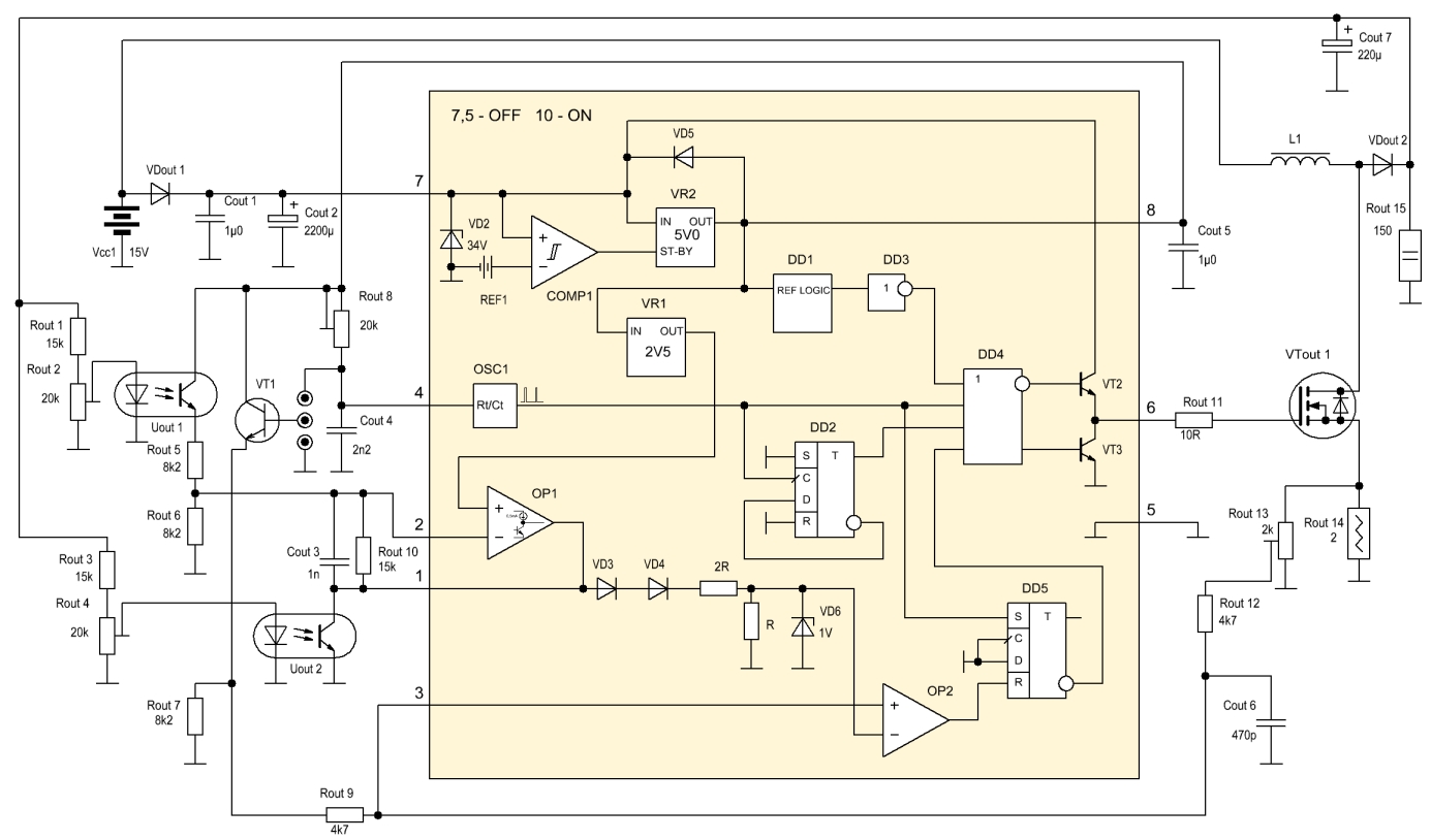
Now we can talk about the microcircuit itself, or more precisely about the principle of its operation. The figure below shows the block diagram of UC3845, i.e. with an internal trigger that does not allow the duration of the control pulse to be more than 50% of the period:
By the way, if you click on the picture, it will open in a new tab. It’s not entirely convenient to jump between tabs, but in any case it’s more convenient than turning the mouse wheel back and forth, returning to the picture that went to the top.
The chip provides dual control of the supply voltage. COMP1 monitors the supply voltage as such and if it is less than the set value, it issues a command that turns the internal five-volt regulator off. If the supply voltage exceeds the switching threshold, the internal stabilizer is unlocked and the microcircuit starts. The second element supervising the power supply is element DD1, which, in cases where the reference voltage differs from the norm, produces a logical zero at its output. This zero goes to inverter DD3 and, transformed into a logical one, goes to logical OR DD4. In almost all block diagrams, this one simply has an inverse input, but I took the inverter outside of this logical element - it’s easier to understand the principle of operation.
The OR logic element works on the principle of determining the presence of a logical one at any of its inputs. That is why it is called OR - if there is a logical one at input 1, OR at input 2, OR at input 3, OR at input 4, then the output of the element will be a logical one.
When a logical one appears at the first input of this adder of all control signals, a logical one will appear at its direct output, and a logical zero will appear at its inverse output. Accordingly, the upper driver transistor will be closed, and the lower one will open, thereby closing the power transistor.
The microcircuit will be in this state until the reference power analyzer gives permission to operate and a logical unit appears at its output, which, after the inverter DD3, unlocks the output element DD4.
Let's say our power supply is normal and the microcircuit starts working. The master oscillator begins to generate control pulses. The frequency of these pulses depends on the values of the frequency-setting resistor and capacitor. There is a slight discrepancy here. The difference doesn’t seem to be big, but nevertheless it exists and there is a possibility of getting something that is not exactly what you wanted, namely a very hot device when a “faster” microcircuit from one manufacturer is replaced with a slower one. The most beautiful picture of the dependence of frequency on the resistance of the resistor and capacitance of the capacitor is from Texas Instruments:
Things are a little different for other manufacturers:

Dependence of frequency on RC ratings of a Fairchild microcircuit

Dependence of frequency on RC ratings of a microcircuit from STMicroelectronics

Dependence of frequency on RC ratings of a microcircuit from UNISONIC TECHNOLOGIES CO
The clock generator produces fairly short pulses in the form of a logical unit. These impulses are divided into three blocks:
1. The same final adder DD4
2. D-trigger DD2
3. RS trigger on DD5
The DD2 trigger is available only in microcircuits of the 44 and 45 subseries. It is this that prevents the duration of the control pulse from becoming longer than 50% of the period, since with each arriving edge of a logical unit from the clock generator it changes its state to the opposite. By doing this, it divides the frequency into two, forming zeros and ones of equal duration.
This happens in a rather primitive way - with each edge arriving at clock input C, the trigger writes to itself the information located at the information input D, and input D is connected to the inverse output of the microcircuit. Due to the internal delay, the inverted information is recorded. For example, the inverting output has a logical zero level. When the edge of the pulse arrives at input C, the trigger manages to record this zero before zero appears at its direct output. Well, if the direct output is zero, then the inverse output will be a logical one. With the arrival of the next edge of the clock pulse, the trigger already writes a logical unit into itself, which will appear at the output after some nanoseconds. Writing a logical one leads to the appearance of a logical zero at the inverse output of the trigger and the process will begin to repeat from the next edge of the clock pulse.

It is for this reason that the UC3844 and UC3845 microcircuits have an output frequency that is 2 times less than that of the UC3842 and UC3843 - it is shared by the trigger.
When the first pulse enters the unit setting input of the RS trigger DD5, it switches the trigger to a state where its direct output is logical one, and its inverse output is zero. And until one appears at input R, trigger DD5 will be in this state.
Suppose we do not have any control signals from the outside, then at the output of the error amplifier OP1 a voltage will appear close to the reference voltage - there is no feedback, the inverting input is in the air, and the non-inverting input is supplied with a reference voltage of 2.5 volts.
Here I’ll make a reservation right away - I personally was somewhat confused by this error amplifier, but after studying the datasheet more carefully and thanks to poking the noses of subscribers, it turned out that the output of this amplifier is not entirely traditional. In the output stage OP1 there is only one transistor connecting the output to the common wire. A positive voltage is generated by a current generator when this transistor is slightly open or completely closed.
From the output of OP1, the voltage passes through a kind of limiter and voltage divider 2R-R. In addition, this same bus has a voltage limit of 1 volt, so that under any conditions more than one volt does not reach the inverting input OP2.
OP2 is essentially a comparator that compares the voltages at its inputs, but the comparator is also tricky - a conventional operational amplifier cannot compare such low voltages - from actual zero to one volt. A conventional op-amp needs either a higher input voltage or a negative side of the supply voltage, i.e. bipolar voltage. The same comparator quite easily copes with the analysis of these voltages; it is possible that there are some biasing elements inside, but before schematic diagram It’s like we don’t really care.
In general, OP2 compares the voltage coming from the output of the error amplifier, or more precisely, the remaining voltage that is obtained after passing through the divider with the voltage at the third pin of the microcircuit (DIP-8 package is meant).
But in this moment We have no time at all on the third pin, and a positive voltage is applied to the inverting input. Naturally, the comparator will invert it and form a clear logical zero at its output, which will not affect the state of the RS trigger DD5 in any way.
As a result of what is happening, we have a logical zero at the first input from the top, DD4, since our power supply is normal, at the second input we have short pulses from the clock generator, at the third input we have pulses from the D-flip-flop DD2, which have the same duration of zero and one . At and at the fourth input we have a logical zero from the RS trigger DD5. As a result, the output of the logic element will completely repeat the pulses generated by the D-trigger DD2. Therefore, as soon as a logical one appears at the direct output of DD4, transistor VT2 will open. At the same time, the inverse output will have a logical zero and transistor VT1 will be closed. As soon as a logical zero appears at the DD4 output, VT2 closes, and the inverse output of DD4 opens VT1, which will be the reason for opening the power transistor.
The current that VT1 and VT2 can withstand is one ampere, therefore this microcircuit can successfully control relatively powerful MOSFET transistors without additional drivers.
In order to understand exactly how the processes occurring in the power supply are regulated, the simplest booster was assembled, since it requires the least number of winding parts. The first GREEN ring that came to hand was taken and 30 turns were wound on it. The quantity was not calculated at all, just one layer of winding was wound and nothing more. I wasn’t worried about consumption - the microcircuit operates in a wide range of frequencies and if you start with frequencies under 100 kHz, then this will be quite enough to prevent the core from entering saturation.
The result was the following booster circuit:
 |
All external elements have the prefix out, meaning that they are OUTSIDE microcircuit details.
I’ll immediately describe what’s on this diagram and why.
VT1 - the base is essentially in the air, the ends are soldered on the board for putting on jumpers, i.e. the base is connected either to ground or to a saw generated by the chip itself. There is no resistor Rout 9 on the board - I even missed its necessity.
Optocoupler Uout 1 uses the error amplifier OP1 to adjust the output voltage, the degree of influence is regulated by resistor Rout 2. Optocoupler Uout 2 controls the output voltage bypassing the error amplifier, the degree of influence is regulated by resistor Rout 4. Rout 14 is a current measuring resistor, specially taken at 2 Ohms so as not to remove the power transistor. Rout 13 - adjusting the current limit threshold. Well, Rout 8 - adjusting the clock frequency of the controller itself.
The power transistor is something that was soldered out of a car converter that was once being repaired - one arm flared up, I changed all the transistors (why ALL the answer is HERE), and this is, so to speak, a surrender. So I don’t know what it is - the inscription is very worn, in general it’s something like 40-50 amperes.
Rout 15 type load - 2 W at 150 Ohm, but 2 W turned out to be not enough. You need to either increase the resistance or increase the power of the resistor - it starts to stink if it works for 5-10 minutes.
VDout 1 - to exclude the influence of the main power on the operation of the controller (HER104 seems to have been a hit), VDout 2 - HER308, well, so that it doesn’t immediately go off if something goes wrong.
I realized the need for resistor R9 when the board was already soldered. In principle, this resistor will still need to be selected, but this is purely optional for those who REALLY want to get rid of the relay method of stabilization at idle. More on this a little later, but for now I stuck this resistor on the side of the tracks:
![]()
First start - engines ALL interlinear connectors must be connected to ground, i.e. they do not affect the circuit. The Rout 8 engine is installed so that the resistance of this resistor is 2-3 kOhm, since the capacitor is 2.2 nF, the frequency should be about 300-odd kHz, therefore at the output of the UC3845 we will get somewhere around 150 kHz.
We check the frequency at the output of the microcircuit itself - this is more accurate, since the signal is not cluttered by shock processes from the inductor. To confirm the differences between the generation frequency and the conversion frequency, we turn the yellow ray to pin 4 and see that the frequency is 2 times higher. The operating frequency itself turned out to be 146 kHz:
Now we increase the voltage on the optocoupler LED Uout 1 in order to control the change in stabilization modes. Here it should be recalled that the resistor Rout 13 slider is in the lower position in the diagram. A common wire is also supplied to the VT1 base, i.e. Absolutely nothing happens at pin 3 and comparator OP2 does not respond to the non-inverting input.
By gradually increasing the voltage on the optocoupler LED, it becomes obvious that control pulses simply begin to disappear. By changing the scan this becomes most clear. This happens because OP2 only monitors what is happening at its inverting input and as soon as the output voltage of OP1 drops below the threshold value, OP2 forms a logical one at its output, which sets trigger DD5 to zero. Naturally, but a logical one appears at the inverse output of the trigger, which blocks the final adder DD4. Thus the microcircuit stops completely.
But the booster is loaded, therefore the output voltage begins to decrease, the Uout 1 LED begins to decrease brightness, the Uout 1 transistor closes and OP1 begins to increase its output voltage and as soon as it passes the OP2 response threshold, the microcircuit starts again.
In this way, the output voltage is stabilized in relay mode, i.e. the microcircuit generates control pulses in batches.
By applying voltage to the LED of the optocoupler Uout 2, the transistor of this optocoupler opens slightly, entailing a decrease in the voltage supplied to the comparator OP2, i.e. the adjustment processes are repeated, but OP1 no longer takes part in them, i.e. the circuit is less sensitive to changes in output voltage. Thanks to this, the control pulse packets have a more stable duration and the picture seems more pleasant (even the oscilloscope is synchronized):
We remove the voltage from the Uout 2 LED and, just in case, check for the presence of a saw on the upper terminal of R15 (yellow beam):

The amplitude is slightly more than a volt and this amplitude may not be enough, because there are voltage dividers on the circuit. Just in case, we unscrew the slider of the tuning resistor R13 to the upper position and control what is happening at the third pin of the microcircuit. In principle, hopes were fully justified - the amplitude is not enough to start limiting the current (yellow ray):
Well, if there is not enough current through the inductor, it means either many turns or a high frequency. Rewinding is too lazy, because the board has a trimming resistor Rout8 to adjust the frequency. We rotate its regulator until the required voltage amplitude is obtained at pin 3 of the controller.
In theory, as soon as the threshold is reached, that is, as soon as the voltage amplitude at pin 3 becomes not much more than one volt, the duration of the control pulse will begin to be limited, since the controller is already beginning to think that the current is too high and it will turn off the power transistor.
Actually, this begins to happen at a frequency of about 47 kHz, and further decreases in frequency had virtually no effect on the duration of the control pulse.
A distinctive feature of the UC3845 is that it controls the flow through the power transistor at almost every cycle of operation, and not the average value, as for example the TL494 does, and if the power supply is designed correctly, then it will never be possible to damage the power transistor...
Now we raise the frequency until the current limitation ceases to have an effect, however, we will make a reserve - we set it to exactly 100 kHz. The blue ray still shows control pulses, but we put the yellow one on the LED of the optocoupler Uout 1 and begin to rotate the trimmer resistor knob. For some time, the oscillogram looks the same as during the first experiment, however, a difference also appears; after passing the control threshold, the duration of the pulses begins to decrease, i.e., real regulation occurs through pulse width modulation. And this is just one of the tricks of this microcircuit - as a reference saw for comparison, it uses a saw that is formed on the current-limiting resistor R14 and thus creates a stabilized voltage at the output:
The same thing happens when the voltage on the optocoupler Uout 2 increases, although in my version it was not possible to get the same short pulses as the first time - the brightness of the optocoupler LED was not enough, and I was too lazy to reduce the resistor Rout 3.
In any case, PWM stabilization occurs and is quite stable, but only in the presence of a load, i.e. the appearance of a saw, not even of great importance, there are 3 controllers on pin. Without this saw, stabilization will be carried out in relay mode.
Now we switch the base of the transistor to pin 4, thereby forcibly feeding the saw to pin 3. There is not a big stumble here - for this feint you will have to select a Rout 9 resistor, since the amplitude of the dust and the level of the constant component turned out to be somewhat too large for me.

However, now the principle of operation itself is more interesting, so we check it by lowering the Rout 13 trimmer engine to the ground and begin to rotate Rout 1.
There are changes in the duration of the control pulse, but they are not as significant as we would like - the large constant component has a strong effect. If you want to use this inclusion option, you need to think more carefully about how to organize it correctly. Well, the picture on the oscilloscope is as follows:
With a further increase in voltage on the optocoupler LED, a breakdown occurs in the relay mode of operation.
Now you can check the load capacity of the booster. To do this, we introduce a limitation on the output voltage, i.e. Apply a small voltage to the Uout 1 LED and reduce the operating frequency. The sociogram clearly shows that the yellow ray does not reach the level of one volt, i.e. There is no current limit. The limitation is provided only by adjusting the output voltage.
In parallel with the load resistor Rour 15, we install another 100 Ohm resistor and the oscillogram clearly shows an increase in the duration of the control pulse, which leads to an increase in the time of energy accumulation in the inductor and its subsequent release to the load:
It is also not difficult to notice that by increasing the load, the voltage amplitude at pin 3 also increases, since the current flowing through the power transistor increases.
It remains to see what happens at the drain in stabilization mode and in its complete absence. We turn a blue beam onto the drain of the transistor and remove the feedback voltage from the LED. The oscillogram is very unstable, since the oscilloscope cannot determine which edge it should synchronize with - after the pulse there is quite a decent “chatter” of self-induction. The result is the following picture.
The voltage on the load resistor also changes, but I won’t make a GIF - the page is already quite “heavy” in terms of traffic, so I declare with full responsibility that the voltage on the load is equal to the voltage maximum value in the picture above minus 0.5 volts.
LET'S SUM IT UP
UC3845 is a universal self-clocking driver for single-ended voltage converters, can work in both flyback and forward converters.
Can operate in relay mode, can operate in full-fledged PWM voltage stabilizer mode with current limitation. It is precisely a limitation, since during an overload the microcircuit goes into current stabilization mode, the value of which is determined by the circuit designer. Just in case, a small sign showing the dependence of the maximum current on the value of the current-limiting resistor:
| I, A | 1 | 1,2 | 1,3 | 1,6 | 1,9 | 3 | 4,5 | 6 | 10 | 20 | 30 | 40 | 50 |
| R, Ohm | 1 | 0,82 | 0,75 | 0,62 | 0,51 | 0,33 | 0,22 | 0,16 | 0,1 | 0,05 | 0,033 | 0,025 | 0,02 |
| 2 x 0.33 | 2 x 0.1 | 3 x 0.1 | 4 x 0.1 | 5 x 0.1 | |||||||||
| P,W | 0,5 | 1 | 1 | 1 | 1 | 2 | 2 | 5 | 5 | 10 | 15 | 20 | 25 |
For full PWM voltage regulation, the IC requires a load because it uses a ramp voltage to compare with the controlled voltage.
Voltage stabilization can be organized in three ways, but one of them requires an additional transistor and several resistors, and this conflicts with the formula LESS PARTS - MORE RELIABILITY, so two methods can be considered basic:
Using an integrated error amplifier. In this case, the feedback optocoupler transistor is connected by the collector to a reference voltage of 5 volts (pin 8), and the emitter supplies voltage to the inverting input of this amplifier through the OS resistor. This method is recommended for more experienced designers, since if the gain of the error amplifier is high, it may become excited.
Without using an integrated error amplifier. In this case, the collector of the regulating optocoupler is connected directly to the output of the error amplifier (pin 1), and the emitter is connected to the common wire. The input of the error amplifier is also connected to the common wire.
The operating principle of PWM is based on monitoring the average output voltage and maximum current. In other words, if our load decreases, the output voltage increases, and the saw amplitude on the current-measuring resistor drops and the pulse duration decreases until the lost balance between voltage and current is restored. As the load increases, the controlled voltage decreases and the current increases, which leads to an increase in the duration of the control pulses.
It is quite easy to organize a current stabilizer on the microcircuit, and the control of the flowing current is controlled at each cycle, which completely eliminates overload of the power stage when making the right choice a power transistor and a current-limiting, or more precisely, measuring resistor installed at the source of the field-effect transistor. It is this fact that has made the UC3845 the most popular when designing household welding machines.
UC3845 has quite serious “rake” - the manufacturer does not recommend using the microcircuit at temperatures below zero, so in the manufacture of welding machines it would be more logical to use UC2845 or UC1845, but the latter are in some shortage. UC2845 is slightly more expensive than UC3845, not as catastrophically as domestic sellers indicated (prices in rubles as of March 1, 2017).

The frequency of the XX44 and XX45 microcircuits is 2 times less than the clock frequency, and the coefficient of filling cannot exceed 50%, then it is most favorable for converters with a transformer. But the XX42 and XX43 microcircuits are best suited for PWM stabilizers, since the duration of the control pulse can reach 100%.
Now, having understood the operating principle of this PWM controller, we can return to designing a welding machine based on it...
Any developer may be faced with the problem of creating a simple and reliable power source for the device he is designing. Until recently, this presented a certain difficulty. However, at present there are quite simple circuit solutions and the corresponding element base that make it possible to create switching power supplies using a minimum number of elements.
This article offers readers a description of one of the existing options simple network pulse block nutrition.
Network part of the power supply
The version of the switching power supply we bring to your attention is implemented based on the UC3842 microcircuit. This microcircuit (MC) has become widespread since the second half of the 90s. It implements many different power supplies for TVs, faxes, VCRs and other equipment. The UC3842 gained such popularity due to its low cost, high reliability, simplicity of circuit design and minimal required wiring.
The MC 384x family with minor differences is produced by many manufacturers: UC3842 (Unitrode, Unitra, Solitron, Phillips Semiconductors), KA3842 (Fairchild Semiconductor), DBL3842 (Daewoo), SG3842 (MicroSemi, Silicon General), TL3842 (Texas Instruments), KIA3842 (KEC ), GL3842 (LG) and many others. There are also domestic microcircuits KR1033EU10 and KR1033EU16, which are modified analogues of UC3842/43/44.
A generalized functional diagram of the 384x family of microcircuits is presented in Fig. 1.

Rice. 1.
MCs of the 384x family are available in various packages - DIP8, SOIC8, DIP14, SOIC14. There are minor differences between them, which boil down, for example, to the presence of separate power and ground terminals at the output transistor stage. However, the most popular are MCs in the DIP8 package. In the future, we will consider precisely this execution of the MS. The assignment of the MC 384x family pins is given in table 1.
Table 1. Pin assignment of 3842/3843 family chips
DIP14, S0IC14 | Output name | Output Description |
|
Error amplifier output |
|||
Feedback input |
|||
Current limit signal input |
|||
Input for connection to the setting RC chain |
|||
Common power supply |
|||
Power input |
|||
Internal reference output +5 V (up to 50 mA) |
|||
Common terminal of the output transistor stage |
|||
Power input of the output transistor stage |
|||
Pins are not used |
The microcircuit contains the following main components:
- zener diode limiting the supply voltage (between pins 5 and 7), usually at a voltage of 36 V (for some manufacturers this voltage is different, for example, in the DBL3842A the value is 29);
- comparator 1, the non-inverting input of which is connected to the power supply, and the inverting input is connected to the internal reference voltage source + 16 V (other MS of the family use different values of the reference voltage source). This comparator determines the MS turn-on voltage;
- controlled by the output signal of the comparator COMP1, a reference voltage source Vref (+5 V. a reference voltage source (+5 V), which is connected through a resistive divider by 2 to the non-inverting input of the error amplifier. The inverting input of this amplifier is connected to pin 2, and the output is connected to pin 1;
- an error amplifier, from the output of which the voltage through two diodes and a resistive divider by 3 is supplied to the inverting input of comparator 2, to which a 1 V zener diode is also connected; the second non-inverting input of the comparator is connected to the pin. 3 (Current Sense);
- built-in pulse generator, the input of which is connected to the pin. 4 MS, to which the time-setting RC chain is connected;
The output of comparator 2 is connected to the R input of the PWM trigger.
The generator output is connected to the S input of the PWM trigger; its inverse output is connected to a multi-input OR element, the other inputs of which are connected to the output of comparator 1 and the pulse generator; The outputs of the OR element control a powerful transistor output stage, the output of which is connected to the pin. 6.
The principle of operation of the MS is easier to consider when comparing its functional diagram and the circuit diagram of the network part of the power supply, shown in rice. 2.

Rice. 2
At the input of the power supply there is a mains voltage rectifier, including fuse PR1 for a current of 5 A, varistor P1 for 275 V to protect the power supply from excess voltage in the network, capacitor C1, thermistor R1 for 4.7 Ohm, diode bridge VD1-VD4 for FR157 diodes (2 A, 600 V) and filter capacitor C2 (220 µF x 400 V). Thermistor R1 in a cold state has a resistance of 4.7 Ohms, and when the power is turned on, the charge current of capacitor C2 is limited by this resistance. Next, the resistor heats up due to the current passing through it, and its resistance drops to tenths of an ohm. However, it has virtually no effect on the further operation of the circuit.
The increasing voltage on the filter capacitor C2 leads to a charge of the capacitor C7 through the resistor R7. The charge current is quite small and does not exceed 3...5 mA. When the voltage on capacitor C7 reaches a level of 16 V (the response threshold of the first comparator, determined by the voltage value of the internal reference voltage source connected to the inverting input of the comparator), the comparator is turned on and a high level. It should be noted that the comparator has hysteresis, i.e. the operation voltage is 16 V, and the turn-off voltage is 10 V for MS 3842 (for 3843 - 8.4 V and 7.6 V, respectively). While the comparator is not turned on, the low level at its output blocks the OR element and the output transistor stage (controlling field-effect transistor VT1), which is closed at this time. When comparator 1 is turned on, its high output voltage turns on the +5 V reference (Vref) and enables the OR gate.
When the reference voltage source is turned on, the built-in generator begins to produce narrow positive rectangular pulses, the frequency of which is determined by the R4C5 elements and which are supplied to the S input of the PWM trigger and the third input of the OR element. These pulses through the OR element (and, accordingly, the transistor output stage) open field-effect transistor VT1. The current through VT1, the primary winding W1 of transformer T1 and resistor R11 begins to increase. The voltage from resistor R11, proportional to the flowing current, is supplied through the integrating chain R10C10 to input 3 of the MS (non-inverting input of comparator 2). Since the converter has not yet reached the operating mode (has not started), capacitor C8 has not yet charged, and its voltage is less than the voltage on capacitor C7.
Therefore, diode VD5 is still closed. Capacitor C7 loses voltage at the moment of the pulse, and when it reaches the switch-off voltage, comparator 1 will turn off (due to hysteresis). The voltage from capacitor C7 through divider R2R3 goes to the inverting input of the error amplifier. It turns out to be below 2.5 V, obtained at the non-inverting input of the error amplifier by dividing the reference voltage (+5 V) by two (on the internal resistors R-R). As a consequence, the voltage at the output of the error amplifier is high, and the zener diode at the inverting input of comparator 2 is turned on through the 2R-R divider. As soon as the voltage at the source of transistor VT1 exceeds 1 V, comparator 2 will turn on and reset the PWM trigger at the R input. The output stage turns off, therefore, transistor VT1 turns off.
Since the resistance of resistor R7 is quite high, during one described startup cycle, capacitor C7 manages to discharge, and capacitor C8 in the feedback winding circuit W2 manages to recharge a little through the diode VD6. Starting attempts will be repeated until the voltage on capacitor C8 exceeds the voltage on capacitor C7. Then the diode VD5 will open, and the feedback winding will begin to power the MS. The frequency of startup attempts is determined by the time constant of the R7C7 elements.
As soon as the voltage at the divider R2R3 exceeds 2.5 V, the voltage at the output of the error amplifier will decrease and the zener diode will turn off. A stabilization mode will begin for the feedback winding, and therefore for all other windings. In this mode, any decrease in voltage in the feedback circuit and on the divider R2R3 causes an increase in voltage at the output of the error amplifier and at the inverting input of the comparator COMP2, and therefore an increase in the current through the field-effect transistor VT1 and the primary winding W1 of transformer T1 and an increase in the transmitted power, and therefore increasing output voltages. Obviously, reducing the voltage in the feedback circuit will have the opposite effect.
Let us note some features of the elements used.
1
. From the above description it follows that the measuring resistor R11 actually sets the possible maximum current through the field-effect transistor VT1. So, with a maximum current of 2 A, its rating should be 0.51 Ohm. at a maximum current of 1 A - correspondingly 1 Ohm, etc. The recommended type of resistor is C5-16MV.
2
. Despite. that inside the MS there is a zener diode that limits the maximum voltage on the pin. 7 (power), in especially critical power supplies it is recommended to install a powerful additional external zener diode of approximately 22...24 V.
3
. The frequency response correction elements of the error amplifier R5C6 should be installed in accordance with the specified ratings, and the capacitance of capacitor C6 is especially critical and should be in the range of 91... 110 pF.
4
. The elements of the timing circuit R4C5 determine the frequency of the internal pulse generator. This frequency can vary over a fairly wide range and reach 250 kHz. It is advisable to use capacitor C5 with high resistance DC. The ratio of the elements of the RC chain can be different, however, with large values of R and small values of C, the control range is much greater than with small values of R and large values of C. The optimal capacitor capacitances are from 2700 to 5100 pF and resistor values from 91 to 130 kOhm.
5
. It should be noted that the common wire of the network part is virtual; in no case should it be connected to the output common wire of the power supply or the product body.

Core and frame ETD39 from Siemens+Matsushita.

Transformer on an ETD39 frame from Siemens+Matsushita.
table 2. Parameters of diodes and their possible replacement
Position | Current, A | Voltage, V | Notes |
||
Pulse diodes |
|||||
Low frequency diodes for general use |
|||||
Pulse diodes |
|||||
Schottky diodes |
Table 3. Field-effect transistor parameters
Conductivity | Ultimate voltage | Maximum current. A | Power, | Resistance open transistor, Ohm | Type of shell |
||
Table 4. Winding data of transformer T1
Contact | Purpose | Wires | Coils | Limit current, A | Voltage single progress. IN |
|
Primary W1 | ||||||
Reverse W2 | ||||||
W4 for +15/12V | ||||||
W5 for -15/12V |
In conclusion, it should be noted that when debugging the network part, it is recommended to remember safety measures, since the elements of the network part of the converter are galvanically connected to the network. It is not recommended to turn on the network part separately without load: this can lead to a significant increase in voltage on individual elements and their breakdown.
The output part of the power supply is shown in rice. 3. It is galvanically isolated from the input part and includes three functionally identical blocks, consisting of a rectifier, an LC filter and a linear stabilizer.

Rice. 3
The first block - a 5 V (5 A) stabilizer - is made on the MS linear stabilizer A2 SD1083/84 (DV, LT). This microcircuit has a switching circuit, housing and parameters similar to the KR142EN12 MS, however, the operating current is 7.5 A for 1083 and 5 A for 1084. The domestic analogue is KR142EN22.
The second block stabilizer +12/15 V (1 A) is made on the MS linear stabilizer A3 7812 (12 V) or 7815 (15 V). Domestic analogues of these MS are KR142EN8 with the corresponding letters (B, V), as well as K1157EN12/15.
The third block - stabilizer -12/15 V (1 A) - is made on the MS linear stabilizer A4 7912 (12 V) or 7915 (15 V). Domestic analogues of these MS-K1162EN12/15.
Resistors R14, R17, R18 are necessary to dampen excess voltage at idle. Capacitors C12, C20, C25 were selected with a voltage reserve due to a possible increase in voltage at idle. It is recommended to use capacitors C17, C18, C23, C28 type K53-1A or K53-4A. All MS are installed on individual plate radiators with an area of at least 5 cm2.
Structurally, the power supply is made in the form of one single-sided printed circuit board installed in the case from the power supply of a personal computer. The fan and network input connectors are used for their intended purpose. The fan is connected to a +12/15V stabilizer, although it is possible to make an additional +12V rectifier or stabilizer without much filtering. All radiators are installed vertically, perpendicular to the air flow exiting through the fan. Four wires 30...45 mm long are connected to the outputs of the stabilizers; each set of output wires is crimped with special plastic clamps-straps into a separate bundle and is equipped with a connector of the same type that is used in a personal computer to connect various peripheral devices.
In conclusion, it should be noted that the transformer has terminals for two more windings, and with careful tight winding, another 1/3 of the free window area remains, so that, if necessary, the range of voltages can be easily expanded.
The stabilization parameters are determined by the parameters of the MS stabilizers. The ripple voltages are determined by the parameters of the converter itself and are approximately 0.05% for each stabilizer.
Oleg Nikolaychuk
Literature
Tue, 04/06/2013 - 23:38 - zival
PWM UC3842AN
The UC3842 is a PWM controller circuit with current and voltage feedback for controlling the key stage of an n-channel MOSFET, providing the discharge of its input capacitance with a forced current of up to 0.7A. The SMPS controller chip consists of a series of UC384X (UC3843, UC3844, UC3845) PWM controller chips. The UC3842 core is specifically designed for long-term operation with a minimum number of external discrete components. The UC3842 PWM controller features precise duty cycle control, temperature compensation, and is low cost. A special feature of the UC3842 is its ability to operate within 100% duty cycle (for example, the UC3844 operates with a duty cycle of up to 50%.). The domestic analogue of UC3842 is 1114EU7. Power supplies made on the UC3842 chip are characterized by increased reliability and ease of implementation.
Rice. Table of standard ratings.
This table gives a complete picture of the differences between the UC3842, UC3843, UC3844, UC3845 microcircuits.
General description.
For those wishing to become more deeply acquainted with the UC384X series PWM controllers, the following material is recommended.
- Datasheet UC3842B (download)
- Datasheet 1114EU7 domestic analogue of the UC3842A microcircuit (download).
- Article "Flyback converter", Dmitry Makashev (download).
- Description of the operation of UCX84X series PWM controllers (download).
- Article "Evolution of flyback switching power supplies", S. Kosenko (download). The article was published in the magazine "Radio" No. 7-9 for 2002.
A document from STC SIT, the most successful description in Russian for PWM UC3845 (K1033EU16), is highly recommended for review. (Download).
The difference between the UC3842A and UC3842B chips is that A consumes less current until startup.
UC3842 has two housing options: 8pin and 14pin, the pinouts of these versions are significantly different. In what follows, only the 8pin housing option will be considered.
A simplified block diagram is necessary to understand the operating principle of a PWM controller.
Rice. Block diagram of UC3842
A block diagram in a more detailed version is necessary for diagnosing and checking the performance of the microcircuit. Since we are considering the 8pin design, Vc is 7pin, PGND is 5pin.
Rice. Block diagram of UC3842 (detailed version)
Rice. UC3842 pinout
There should be material on pin assignments here, but it is much more convenient to read and look at the practical circuit diagram for connecting the UC3842 PWM controller. The diagram is drawn so well that it makes it much easier to understand the purpose of the microcircuit pins.
Rice. Connection diagram of UC3842 using the example of a power supply for TV
1. Comp:(Russian Correction) error amplifier output. For normal operation of the PWM controller, it is necessary to compensate for the frequency response of the error amplifier; for this purpose, a capacitor with a capacity of about 100 pF is usually connected to the specified pin, the second pin of which is connected to pin 2 of the IC. If the voltage at this pin is lowered below 1 volt, then the pulse duration at output 6 of the microcircuit will decrease, thereby reducing the power of this PWM controller.
2. Vfb: (Russian) Feedback voltage) feedback input. The voltage at this pin is compared with a reference voltage generated inside the UC3842 PWM controller. The comparison result modulates the duty cycle of the output pulses, as a result the output voltage of the power supply is stabilized. Formally, the second pin serves to reduce the duration of the output pulses; if it is applied above +2.5 volts, the pulses will be shortened and the microcircuit will reduce the output power.
3. C/S: (second designation I sense) (Russian) Current feedback) current limit signal. This pin must be connected to a resistor in the source circuit of the switching transistor. When the MOS transistor is overloaded, the voltage across the resistance increases and when a certain threshold is reached, the UC3842A stops operating, closing the output transistor. Simply put, the pin serves to turn off the pulse at the output when a voltage above 1 volt is applied to it.
4. Rt/Ct: (Russian) Frequency setting) connection of a timing RC circuit necessary to set the frequency of the internal oscillator. R is connected to Vref - the reference voltage, and C is connected to the common wire (usually several tens of nF are selected). This frequency can be changed within a fairly wide range; from above it is limited by the speed of the key transistor, and from below by the power of the pulse transformer, which decreases with decreasing frequency. In practice, the frequency is selected in the range of 35...85 kHz, but sometimes the power supply works quite normally at a much higher or much lower frequency.
For a timing RC circuit, it is better to abandon ceramic capacitors.
5.Gnd: (Russian) General) general conclusion. The common terminal should not be connected to the circuit body. This “hot” ground is connected to the device body through a pair of capacitors.
6.Out: (Russian) Exit) the output of the PWM controller is connected to the gate of the switching transistor through a resistor or a resistor and diode connected in parallel (anode to the gate).
7.Vcc: (Russian) Nutrition) power input of the PWM controller, this pin of the microcircuit is supplied with a supply voltage in the range from 16 volts to 34, please note that this microcircuit has a built-in Schmidt trigger (UVLO), which turns on the microcircuit if the supply voltage exceeds 16 volts, if the voltage for some reason it drops below 10 volts (for other microcircuits of the UC384X series, the ON/OFF values may differ, see the Table of Type Ratings), it will be disconnected from the supply voltage. The microcircuit also has overvoltage protection: if the supply voltage on it exceeds 34 volts, the microcircuit will turn off.
8. Vref: output of the internal reference voltage source, its output current is up to 50 mA, voltage 5 V. Connected to one of the divider arms, it is used to quickly adjust the U output of the entire power supply.
A little theory.
Rice. Shutdown circuit when input voltage drops.
The Under-Voltage LockOut circuit, or UVLO circuit, ensures that Vcc is equal to the voltage that makes the UC384x fully operational to turn on the output stage. In Fig. It is shown that the UVLO circuit has turn-on and turn-off threshold voltages of 16 and 10, respectively. Hysteresis of 6V prevents random switching on and off of voltage during power supply.
Generator.
Rice. Generator UC3842.
The frequency-setting capacitor Ct is charged from Vref (5V) through the frequency-setting resistor Rt, and discharged by an internal current source.
The UC3844 and UC3845 chips have a built-in counting trigger, which serves to obtain a maximum generator duty cycle of 50%. Therefore, the generators of these microcircuits must be set to a switching frequency twice as high as desired. The UC3842 and UC3843 chip generators are set to the desired switching frequency. The maximum operating frequency of the UC3842/3/4/5 family of generators can reach 500 kHz.
Reading and limiting current.
Rice. Organization of current feedback.
The current-voltage conversion is performed on an external resistor Rs connected to ground. RC filter to suppress output switch emissions. The inverting input of the UC3842 current-sensing comparator is internally biased by 1V. Current limiting occurs if the voltage at pin 3 reaches this threshold.
Rice. Block diagram of an error signal amplifier.
The non-inverting error input does not have a separate output and is internally biased by 2.5 volts. The output of the error amplifier is connected to pin 1 to connect an external compensating circuit, allowing the user to control the frequency response of the converter's closed feedback loop.
Rice. Compensating circuit diagram.
A compensating circuit suitable for stabilizing any converter circuit with additional current feedback, except flyback and boost converters operating with inductor current.
Blocking methods.
There are two possible ways to block the UC3842 chip:
increasing the voltage at pin 3 above the level of 1 volt,
or raising the voltage at pin 1 to a level not exceeding the voltage drop across the two diodes relative to ground potential.
Each of these methods results in setting a HIGH logic voltage level at the output of the PWM coparator (block diagram). Since the main (default) state of the PWM latch is the reset state, the output of the PWM comparator will be held LOW until the state of pins 1 and/or 3 changes in the next clock period (the period that follows the one in question). clock period when a situation arose that required blocking the microcircuit).
Connection diagram.
The simplest scheme connecting the UC3842 PWM controller is purely academic in nature. The circuit is the simplest generator. Despite its simplicity, this scheme works.
Rice. The simplest connection diagram 384x
As can be seen from the diagram, for the UC3842 PWM controller to operate, only an RC circuit and power are required.
Connection diagram for the PWM controller of the UC3842A PWM controller, using the example of a TV power supply.
Rice. Power supply diagram for UC3842A.
The diagram gives a clear and simple representation of the use of the UC3842A in a simple power supply. The diagram has been slightly modified to make it easier to read. The full version of the circuit can be found in the PDF document "Power supplies 106 circuits" Tovarnitsky N.I.
Connection diagram of the PWM controller of the UC3843 PWM controller, using the example of the power supply of the D-Link router, JTA0302E-E.
Rice. Power supply diagram for UC3843.
Although the circuit is made according to the standard connection for the UC384X, however, R4 (300k) and R5 (150) are taken out of the standards. However, successfully, and most importantly, logically allocated circuits help to understand the principle of operation of the power supply.
Power supply based on the UC3842 PWM controller. The diagram is not intended to be repeated, but is for informational purposes only.
Rice. Standard connection diagram from the datasheet (the diagram has been slightly modified for easier understanding).
Repair of PWM-based power supply UC384X.
Checking using an external power supply.
Rice. Simulation of PWM controller operation.
The operation is checked without unsoldering the microcircuit from the power supply. Before carrying out diagnostics, the power supply must be disconnected from the 220V network!
From an external stabilized power supply, apply a voltage to pin 7 (Vcc) of the microcircuit with a voltage greater than the UVLO turn-on voltage, in general more than 17V. In this case, the UC384X PWM controller should work. If the supply voltage is less than the UVLO turn-on voltage (16V/8.4V), the microcircuit will not start. You can read more about UVLO here.
Checking the internal voltage reference.
For a working UC384X PWM controller, the voltage at pin 8(Vref) should be +5V.
ExaminationUVLO
If the external power supply allows you to regulate the voltage, then it is advisable to check the operation of the UVLO. By changing the voltage on pin 7(Vcc) within the UVLO voltage range, the reference voltage on pin 8(Vref) = +5V should not change.
UC3842 and UC3844 turn-on voltage 16V, turn-off voltage 10V
UC3843 and UC3845 turn-on voltage 8.4V, turn-off voltage 7.6V
It is not recommended to supply a voltage of 34V or higher to pin 7 (Vcc). It is possible that there is a protective zener diode in the power supply circuit of the UC384X PWM controller, then it is not recommended to supply this zener diode above the operating voltage.
Checking the operation of the generator and external circuits of the generator.
You will need an oscilloscope to check. There should be a stable “saw” at pin 4(Rt/Ct).
Checking the output control signal.
You will need an oscilloscope to check. Ideally, pin 6(Out) should have rectangular pulses. However, the circuit under study may differ from the one shown, and then it will be necessary to turn off the external feedback circuits. The general principle is shown in Fig. - with this activation, the UC384X PWM controller is guaranteed to start.
Rice. Operation of UC384x with feedback circuits disabled.
Rice. An example of real signals when simulating the operation of a PWM controller.
If a power supply with a control PWM controller such as UC384x does not turn on or turns on with a long delay, then check by replacing the electrolytic capacitor that filters the power supply (pin 7) of this m/s. It is also necessary to check the elements of the initial start circuit (usually two 33-100kOhm resistors connected in series).
When replacing a power (field-effect) transistor in a power supply unit with a control m/s 384x, be sure to check the resistor that serves as a current sensor (located at the source of the field-effect switch). A change in its resistance at a nominal fraction of an ohm is very difficult to detect with a conventional tester! An increase in the resistance of this resistor leads to false operation of the current protection of the power supply unit. In this case, you can look for a very long time for the reasons for the power supply overload in the secondary circuits, although they are not there at all.
Comments
Sat, 10/08/2013 - 00:24 - vitaly
Hello, writing to you
Hello
Vitaly writes to you
I'm from Ukraine
I kindly ask you to help with advice on the UC3845 (SOIC-14) chip
I repair industrial electronics
in one device this series is used in a power supply unit - UC3844 - this is for startup,
and in the secondary there is UC3845
question specifically about 3845
on the board there is a UC3845 (without the letter at the end) - and in the diagram for this device
the manufacturer writes that UC3845 should be with the letter (D)
There are no such microcircuits in such a package with the letter (D) anywhere
-there is UC3845BDG
-and there is UC3845AD
but neither has twice the difference in price
I wanted to know what the letter after the numbers means
I looked through all the datasheets and nothing intelligible
tell me please
Vitaly
Sat, 10/08/2013 - 00:34 - zival
UC3845BDG and UC3845ADLet's start with
UC3845BDG and UC3845AD
Let's begin with
UC3845 is a series of chips, PWM controllers in the general case (in fact, it is an 84 series of PWM controllers).
UC3845B UC3845A letter A characterizes a reduced starting current, that is, for
UC3845B inrush current 1mA
UC3845A starting current 0.5mA
In most cases the difference is negligible. Formally, if we neglect many factors, one resistor is installed to power the UC3845A, and two resistors connected in parallel are installed to power the UC3845B, meaning the initial start-up. In your case, for an accurate answer, tell me what you have in the initial start-up power circuit - one or two resistors, or the value of this resistor (R4 300k in the figure below).
UC3845x D The letter D denotes the package type, that is, the SOIC package type. You should pay attention to the fact that the type of package is not indicated on the microcircuit case, but in the PART NUMBER (catalog designation) the designation is simply necessary, for example D-8 is a SOIC-8 package (8 legs, planar design) simply D - This is a SOIC-16 package (16 legs, planar design). In your case, UC3845x D stands for planar design SOIC-16 package.
UC3845xx G The letter G means that there is no lead in the chip, which means that the chip will not pollute when disposed of environment. This letter is very important if you want to certify (for sale for commercial purposes) your self-assembled device with certification bodies. By law, you must protect the environment; the use of microcircuits with the letter G allows you to do this, however, at the expense of increasing the price of the product.
Conclusion: Both of the listed microcircuits will suit you. If you don’t know the current consumption at start-up or are too lazy to count, and you also have doubts about what to take, take a microcircuit with the letter A, you won’t go wrong. If you are a fighter for a clean environment, then take it with the letter G.
Source. Description of the operation of UCX84X series PWM controllers ().
Mon, 11/11/2013 - 02:04 - zival
In principle it is possible, but that's all
In principle, it is possible, but this is still a specialized PWM for the power supply, and it is in the power supplies that all the potential inherent in it is revealed. Using the generic 555 academically is much easier. Everything there is clear, open and easier to understand.
Wed, 14/08/2013 - 11:42 - Guest
Hello
Hello Valery.
The 36V charger of a children's electric car has stopped working.
Charger collected on UC3842A.
The field worker unsoldered and applied 20V to the 7th leg.
1 leg - 5V
2nd leg - 2.5V (or short to ground)
3rd leg - 0V (or short to ground)
4 leg - saw
5th leg - earth
7 leg - 20V
On the 6th leg 0 (I look with an oscilloscope)
What is the reason, please help my granddaughter drive a car.
Wed, 14/08/2013 - 13:17 - zival
Most likely the PWM controller is faulty
1. The 2.5 volts on the 2nd leg is somewhat confusing, it is advisable to short it to ground.
2. With the power supply disconnected from all voltages, use an ohmmeter to measure the resistance between the 6th leg of the microcircuit and the ground (5th leg), also between the 6th leg of the microcircuit and the power supply (7th leg). In both cases, the resistance should be infinite, since the microcircuit has two transistors at the output (6th leg). Let's look block diagram PWM controller.
If there is a short circuit in one or both arms, then the microcircuit is faulty. When checking, you don’t have to unsolder the microcircuit, but it is advisable to unsolder the transistor; if it is short, then the measurements may be erroneous. Although, from experience with the 384X PWM controller, if the power switch burns out, then in 90% of cases the PWM controller itself fails. In fact, it is possible to measure the arms without unsoldering the power switch, if one or both arms are short-circuited - PWM controller 384X and switch are faulty.
3. According to your description, PWM 3842 is faulty, namely the output stage (6th leg) is faulty.
4. I would like to note the fact that 20 volts can swing the power switch, so in principle you can see pulses on the secondary winding of the transformer, although very small. If there are pulses, then the field switch is actually working and the PWM is working. You really need to start PWM first.
Wed, 14/08/2013 - 20:20 - Guest
Hello Valery. Thank you
Hello Valery. Thanks for the answer. Please tell me what can replace the UC3842A MiniDip 8 pin without further settings and modifications to the circuit.
And another question. How to replace 5N60C, otherwise this item is only made to order (I focus on Chip and Dip).
Wed, 14/08/2013 - 21:19 - zival
If I understood correctly about
If I understand correctly about the housing, you are interested in the DIP8 housing. As in the picture.
This is the first time I’ve come across the term MiniDip 8 pin, so I’ll clarify. If the case is like this, then at the end there should be the letter “N”, which designates such a case. For example UC3842AN.
Without modifications, any microcircuit that has a set of numbers 3842 in its name will suit you; if there is the letter “A” immediately after the numbers, then this will be a pleasant bonus (the cost of a microcircuit with or without the letter “A” is the same). For example UC3842 A N
Conclusion. Any microcircuit xx 3842x Nxxxx will suit you, where x is any letter or no letter at all. For example KA3842AN, KA3842N, KA3842BN. These options are only needed when removing a microcircuit from some donor; when purchasing, order exactly the same microcircuit that was installed before.
I think the transistor is a 5N60C case with a metal heatsink (not plastic, plastic has a slightly different marking). This is an ordinary field switch, full name FQP5N60C 4.5A 600V, 2.5Ohm. Any field device with a current of more than 4.5A and a voltage of more than 600V, and a resistance of less than 2.5 ohm, is suitable. For example IRF840.
Hand on heart, there are many analogues, for example, I would do this, go to the Rembyttekhnika store, where we buy parts and type the keyword MOS-N-FET into the search line, then I would run my eyes, selecting only positions containing ONLY phrases “TO220”, “MOS-N-FET” “V-MOS”, then we focus only on the price tag, voltage, current and resistance. Select by parameters The selection principle is described just above italics. For example, the search results for the transistor you need rbt74.ru/search?page=2&search_string=MOS-N-FET&logo I think you’ll figure it out.
Mon, 28/10/2013 - 20:32 - Guest
If the specified transistor
If the specified transistor is an analogue of FQD5N60CTM pdf1.alldatasheet.com/datasheet-pdf/view/533793/FAIRCHILD/FQD5N60CTM.html then it can be replaced with any similar one and even BUZ90 will do, but the reason for the combustion of field-effect transistors is very often associated with the inability of the PWM output stage controller to securely lock the field-effect transistor. Therefore, you should choose a transistor with a high opening threshold voltage at the gate of the field switch for more reliable closing of it. The input capacitance also significantly affects the operating mode of the transistor. The smaller the input capacitance, the easier it is for the PWM controller to turn it on and off. For this reason, I personally do not trust or use circuits without output switch drivers.
Wed, 21/08/2013 - 11:30 - zival
If there is no oscilloscope, but there is
If there is no oscilloscope, but only a multimeter.
1. Check the power supply on leg 7; for UC3845 the voltage should be greater than 8.6 volts. If you change the starting capacitor less, it is easy to find, it sits on the 7th leg and has a rating of 47 µF * 50V (sometimes there is an option of 25V, 63V, 100V), and in general, repairing power supplies on the UC384x begins with replacing the starting capacitor.
2. Check the reference voltage on leg 8, it should be +5V. If not, the microcircuit is faulty; before drawing a conclusion, follow step 1.
3. With the power supply turned off, check the resistance between legs 6 and 5, legs 6 and 7 - in both cases it should not be short.
Tue, 21/01/2014 - 13:25 - Toss
Thank you very much
For clarification of the principles of work and articles with examples and calculations. Just an oasis in the desert. Everything is clear, accessible and intelligible. The datasheet is even in Russian, it’s super!).
I decided to start repairing computer power supplies here - it’s a pity to throw it away, and in the first block I came across this PWM. There is little information, but here is a complete and detailed description). Thanks again for the info!
Fri, 04/25/2014 - 13:56 - Guest (not verified)
good time
Good day.
The problem is the following, I can’t understand what the reason is: I have a power supply from a D link router, the microcircuit is powered through a 300K resistor, on the page it was written somewhere that the current consumption of the microcircuit is 1mA, mine consumes 14 mA, as a result the supply voltage It turns out not enough to start the microcircuit, about 7 volts.
I changed the microcircuit, the picture did not change, the soldered microcircuit consumes about 12 mA. It starts normally from the power supply, and all the signals are there, but it consumes a lot :(
Has anyone had a similar problem?
Fri, 04/25/2014 - 15:46 - zival
No problem, nominal
No problem, rated current consumption is 11 mA, maximum 17 mA, so you are in the range of rated current consumption. The starting current is 0.5 mA (1 mA for letter A), this is a slightly different parameter that is important for self-powered systems. Source
The article is devoted to the design, repair and modification of power supplies wide range equipment based on the UC3842 chip. Some of the information provided was obtained by the author as a result of personal experience and will help you not only avoid mistakes and save time during repairs, but also increase the reliability of the power source. Since the second half of the 90s, a huge number of televisions, video monitors, faxes and other devices have been produced whose power supplies (PS) use the UC3842 integrated circuit (hereinafter - IC). Apparently, this is explained by its low cost, the small number of discrete elements needed for its “body kit” and, finally, the fairly stable characteristics of the IC, which is also important. Variants of this IC produced by different manufacturers may differ in prefixes, but always contain a 3842 core.
As can be seen from the circuit diagram, the power supply is designed for a network voltage of 115 V. The undoubted advantage of this type of power supply is that with minimal modifications it can be used in a network with a voltage of 220 V, you just need to:
- replace the diode bridge connected at the input of the power supply with a similar one, but with reverse voltage 400 V;
- replace the electrolytic capacitor of the power filter, connected after the diode bridge, with one of equal capacity, but with an operating voltage of 400 V;
- increase the value of resistor R2 to 75…80 kOhm;
- check the CT for the permissible drain-source voltage, which must be at least 600 V. As a rule, even in power supplies designed to operate on a 115 V network, CTs capable of operating on a 220 V network are used, but, of course, exceptions are possible. If the CT needs to be replaced, the author recommends the BUZ90.
As mentioned earlier, the IC has some features related to its power supply. Let's take a closer look at them. At the first moment after connecting the IP to the network, the internal generator of the IC is not yet working, and in this mode it consumes very little current from the power circuits. To power the IC in this mode, the voltage obtained from resistor R2 and accumulated on capacitor C2 is sufficient. When the voltage on these capacitors reaches 16...18 V, the IC generator starts and it begins to generate CT control pulses at the output. Voltage appears on the secondary windings of transformer T1, including windings 3-4. This voltage is rectified by pulse diode D3, filtered by capacitor C3, and supplied to the IC power circuit through diode D2. As a rule, a zener diode D1 is included in the power circuit, limiting the voltage to 18...22 V. After the IC has entered the operating mode, it begins to monitor changes in its supply voltage, which is fed through the divider R3, R4 to the feedback input Vfb. By stabilizing its own supply voltage, the IC actually stabilizes all other voltages removed from the secondary windings of the pulse transformer.
When there are short circuits in the circuits of the secondary windings, for example, as a result of breakdown of electrolytic capacitors or diodes, energy losses in the pulse transformer increase sharply. As a result, the voltage obtained from winding 3-4 is not enough to maintain normal operation of the IC. The internal oscillator turns off, a low level voltage appears at the output of the IC, which turns the CT into a closed state, and the microcircuit is again in low power consumption mode. After some time, its supply voltage increases to a level sufficient to start the internal generator, and the process repeats. In this case, characteristic clicks (clicking) are heard from the transformer, the repetition period of which is determined by the values of capacitor C2 and resistor R2.
When repairing power supplies, situations sometimes arise when a characteristic clicking noise is heard from the transformer, but a thorough check of the secondary circuits shows that there is no short circuit in them. In this case, you need to check the power supply circuits of the IC itself. For example, in the author’s practice there were cases when capacitor C3 was broken. Common cause such behavior of the IP is a break rectifier diode D3 or decoupling diode D2.
When a powerful CT breaks down, it usually has to be replaced along with the IC. The fact is that the CT gate is connected to the output of the IC through a resistor of a very small value, and when the CT breaks down, the output of the IC gets high voltage from the primary winding of the transformer. The author categorically recommends that if the CT malfunctions, replace it together with the IC; fortunately, its cost is low. IN otherwise, there is a risk of “killing” the new CT, because if a high voltage level from the broken IC output is present at its gate for a long time, it will fail due to overheating.
Some other features of this IC were noticed. In particular, when a CT breaks down, resistor R10 in the source circuit very often burns out. When replacing this resistor, you should stick to a value of 0.33...0.5 Ohm. Overestimating the resistor value is especially dangerous. In this case, as practice has shown, the first time the power supply is connected to the network, both the microcircuit and the transistor fail.
In some cases, an IP failure occurs due to a breakdown of the zener diode D1 in the IC power circuit. In this case, the IC and CT, as a rule, remain serviceable; it is only necessary to replace the zener diode. If the zener diode breaks, both the IC itself and the CT often fail. For replacement, the author recommends using domestic KS522 zener diodes in a metal case. Having bitten out or removed the faulty standard zener diode, you can solder the KS522 with the anode to pin 5 of the IC and the cathode to pin 7 of the IC. As a rule, after such a replacement, similar malfunctions no longer occur.
You should pay attention to the serviceability of the potentiometer used to adjust the output voltage of the IP, if there is one in the circuit. It is not in the above diagram, but it is not difficult to introduce it by connecting resistors R3 and R4 into the gap. Pin 2 of the IC must be connected to the motor of this potentiometer. I note that in some cases such modification is simply necessary. Sometimes, after replacing the IC, the output voltages of the power supply turn out to be too high or too low, and there is no adjustment. In this case, you can either turn on the potentiometer, as mentioned above, or select the value of resistor R3.
According to the author’s observation, if high-quality components are used in the IP, and it is not operated under extreme conditions, its reliability is quite high. In some cases, the reliability of the power supply can be increased by using resistor R1 of a slightly larger value, for example, 10...15 Ohms. In this case, transient processes when the power is turned on proceed much more calmly. In video monitors and televisions, this must be done without affecting the demagnetization circuit of the kinescope, i.e., the resistor must under no circumstances be connected to the break in the general power circuit, but only to the connection circuit of the power supply itself.
Below are links to various microcircuits analogues of UC3842, which can be purchased from Dalincom UC3842AN dip-8, KA3842A dip-8, KA3842 sop-8, UC3842 sop-8, TL3842P, and others in the power supply microcircuits section.
Alexey Kalinin
"Electronic equipment repair"