Scheme of a switching power supply ATX 68a. Modern ATX power supplies and their characteristics
Introduction
An integral part of every computer is the power supply. It is just as important as the rest of the computer. At the same time, purchasing a power supply is quite rare, because a good power supply can provide power to several generations of systems. Taking all this into account, the purchase of a power supply must be taken very seriously, since the fate of the computer is directly dependent on the performance of the power supply.
To implement galvanic isolation, it is enough to manufacture a transformer with the necessary windings. But powering a computer requires a lot of power, especially for modern PCs. To power the computer, a transformer would have to be made, which would not only be large in size, but also weigh a lot. However, as the frequency of the transformer supply current increases, to create the same magnetic flux, fewer turns and a smaller cross-section of the magnetic core are required. In power supplies built on the basis of a converter, the frequency of the transformer supply voltage is 1000 or more times higher. This allows you to create compact and lightweight power supplies.
The simplest pulse power supply
Consider a block diagram of a simple pulse block power supply, which underlies all switching power supplies.
Block diagram of a switching power supply.
The first block carries out the transformation AC voltage networks permanently. Such a converter consists of a diode bridge that rectifies alternating voltage and a capacitor that smoothes out the ripples of the rectified voltage. This box also contains additional elements: mains voltage filters from pulse generator ripples and thermistors to smooth out the current surge at the moment of switching on. However, these elements may be omitted in order to save on cost.
The next block is a pulse generator, which generates pulses at a certain frequency that power the primary winding of the transformer. The frequency of the generating pulses of different power supplies is different and lies in the range of 30 - 200 kHz. The transformer performs the main functions of the power supply: galvanic isolation from the network and reducing the voltage to the required values.
The alternating voltage received from the transformer is converted by the next block into direct voltage. The block consists of voltage rectifying diodes and a ripple filter. In this block, the ripple filter is much more complex than in the first block and consists of a group of capacitors and a choke. In order to save money, manufacturers can install small capacitors, as well as chokes with low inductance.
The first switching power supply was a push-pull or single-cycle converter. Push-pull means that the generation process consists of two parts. In such a converter, two transistors open and close in turn. Accordingly, in a single-ended converter one transistor opens and closes. Circuits of push-pull and single-cycle converters are presented below.

Schematic diagram converter
Let's take a closer look at the elements of the circuit:
X2 - connector power supply circuit.
X1 is the connector from which the output voltage is removed.
R1 is a resistance that sets the initial small bias on the keys. It is necessary for a more stable start of the oscillation process in the converter.
R2 is a resistance that limits the base current on the transistors; this is necessary to protect the transistors from burning out.
TP1 - The transformer has three groups of windings. The first output winding generates the output voltage. The second winding serves as a load for the transistors. The third generates the control voltage for the transistors.
At the initial moment of turning on the first circuit, the transistor is slightly open, because A positive voltage is applied to the base through resistor R1. A current flows through the slightly open transistor, which also flows through winding II of the transformer. The current flowing through the winding creates a magnetic field. The magnetic field creates voltage in the remaining windings of the transformer. As a result, a positive voltage is created on winding III, which opens the transistor even more. The process continues until the transistor reaches saturation mode. The saturation mode is characterized by the fact that as the applied control current to the transistor increases, the output current remains unchanged.
Since the voltage in the windings is generated only if there is a change magnetic field, its increase or decrease, then the absence of an increase in the current at the output of the transistor will, therefore, lead to the disappearance of the EMF in windings II and III. A loss of voltage in winding III will lead to a decrease in the degree of opening of the transistor. And the output current of the transistor will decrease, therefore, the magnetic field will decrease. Decreasing the magnetic field will create a voltage of opposite polarity. The negative voltage in winding III will begin to close the transistor even more. The process will continue until the magnetic field completely disappears. When the magnetic field disappears, the negative voltage in winding III will also disappear. The process will begin to repeat itself again.
A push-pull converter works on the same principle, but the difference is that there are two transistors, and they open and close in turn. That is, when one is open, the other is closed. The push-pull converter circuit has the great advantage of using the entire hysteresis loop of the magnetic conductor of the transformer. Using only one section of the hysteresis loop or magnetizing in only one direction leads to many undesirable effects that reduce the efficiency of the converter and degrade its performance. Therefore, a push-pull converter circuit with a phase-shifting transformer is generally used everywhere. In circuits where simplicity, small dimensions, and low power are needed, a single-cycle circuit is still used.
ATX form factor power supplies without power factor correction
The converters discussed above, although complete devices, are inconvenient to use in practice. The converter frequency, output voltage and many other parameters “float”, changing depending on changes in: supply voltage, converter output load and temperature. But if the keys control a controller that could carry out stabilization and various additional functions, then you can use the circuit to power the devices. The power supply circuit using a PWM controller is quite simple, and, in general, is a pulse generator built on a PWM controller.
PWM - pulse width modulation. It allows you to adjust the amplitude of the signal passed through the low-pass filter (filter low frequencies) with a change in the duration or duty cycle of the pulse. The main advantages of PWM are the high efficiency of power amplifiers and great application possibilities.

Scheme simple block power supply with PWM controller.
This power supply circuit has a low power and uses a field-effect transistor as a key, which makes it possible to simplify the circuit and get rid of additional elements required to control transistor switches. In high-power power supplies, the PWM controller has control elements (“Driver”) for the output switch. IGBT transistors are used as output switches in high-power power supplies.
The mains voltage in this circuit is converted to DC voltage and supplied through a switch to the first winding of the transformer. The second winding serves to power the microcircuit and generate voltage feedback. The PWM controller generates pulses with a frequency that is set by an RC chain connected to pin 4. The pulses are fed to the input of the switch, which amplifies them. The duration of the pulses varies depending on the voltage on leg 2.
Let's consider a real ATX power supply circuit. It has many more elements and also contains additional devices. The power supply circuit is conventionally divided into main parts by red squares.
ATX power supply circuit with a power of 150-300 W.
To power the controller chip, as well as generate the standby voltage +5, which is used by the computer when it is turned off, there is another converter in the circuit. In the diagram it is designated as block 2. As you can see, it is made according to the circuit of a single-cycle converter. The second block also contains additional elements. Basically, these are chains for absorbing voltage surges that are generated by the converter transformer. Microcircuit 7805 - a voltage stabilizer generates a standby voltage of +5V from the rectified voltage of the converter.
Often, low-quality or defective components are installed in the standby voltage generating unit, which causes the frequency of the converter to decrease to the audio range. As a result, a squeaking sound is heard from the power supply.
Since the power supply is powered from a 220V AC network, and the converter needs power constant voltage, the voltage needs to be converted. The first block rectifies and filters alternating mains voltage. This block also contains a filter against interference generated by the power supply itself.
The third block is the TL494 PWM controller. It carries out all the main functions of the power supply. Protects the power supply from short circuits, stabilizes output voltages and generates a PWM signal to control transistor switches that are loaded on the transformer.
The fourth block consists of two transformers and two groups of transistor switches. The first transformer generates the control voltage for the output transistors. Since the TL494 PWM controller generates a low power signal, the first group of transistors amplifies this signal and passes it to the first transformer. The second group of transistors, or output ones, are loaded onto the main transformer, which generates the main supply voltages. This more complex output switch control scheme was used due to the complexity of control bipolar transistors and protecting the PWM controller from high voltage.
The fifth block consists of Schottky diodes, which rectify the output voltage of the transformer, and a low-pass filter (LPF). The low-pass filter consists of electrolytic capacitors of significant capacity and chokes. At the output of the low-pass filter there are resistors that load it. These resistors are necessary to ensure that the power supply capacity does not remain charged after turning off. There are also resistors at the output of the mains voltage rectifier.
The remaining elements not circled in the block are chains that form “service signals”. These chains protect the power supply from short circuits or monitor the health of the output voltages.

ATX power supply 200 W.
Now let's see how the elements are located on the printed circuit board of a 200 W power supply. The picture shows:
Capacitors that filter output voltages.
Place of unsoldered output voltage filter capacitors.
Inductors that filter the output voltages. The larger coil not only plays the role of a filter, but also acts as a ferromagnetic stabilizer. This allows you to slightly reduce voltage imbalances when the load of different output voltages is uneven.
WT7520 PWM stabilizer chip.
A radiator on which Schottky diodes are installed for voltages +3.3V and +5V, and for voltage +12V there are ordinary diodes. It should be noted that often, especially in older power supplies, additional elements are placed on the same radiator. These are voltage stabilization elements +5V and +3.3V. In modern power supplies, only Schottky diodes are placed on this radiator for all main voltages or field effect transistors, which are used as a rectifying element.
The main transformer, which generates all voltages, as well as galvanic isolation from the network.
A transformer that generates control voltages for the output transistors of the converter.
Converter transformer generating standby voltage +5V.
The radiator on which the output transistors of the converter are located, as well as the transistor of the converter that generates the standby voltage.
Mains voltage filter capacitors. There don't have to be two of them. To form a bipolar voltage and form a midpoint, two capacitors of equal capacity are installed. They divide the rectified mains voltage in half, thereby forming two voltages of different polarities, connected at a common point. In single-supply circuits there is only one capacitor.
Network filter elements against harmonics (interference) generated by the power supply.
Diode bridge diodes that rectify AC mains voltage.

ATX power supply 350 W.
The 350 W power supply is designed equivalently. What immediately catches your eye is the large board size, larger radiators and larger converter transformer.
Output voltage filter capacitors.
A radiator that cools the diodes that rectify the output voltage.
PWM controller AT2005 (analogous to WT7520), which stabilizes voltages.
The main transformer of the converter.
A transformer that generates control voltage for output transistors.
Standby voltage converter transformer.
A radiator that cools the output transistors of the converters.
Mains voltage filter against power supply interference.
Diode bridge diodes.
Mains voltage filter capacitors.
The considered circuit has been used in power supplies for a long time and is now sometimes found.
ATX format power supplies with power factor correction.
In the considered circuits, the network load is a capacitor connected to the network through a diode bridge. The capacitor is charged only if the voltage across it is less than the mains voltage. As a result, the current is pulsed in nature, which has many disadvantages.

Bridge voltage rectifier.
We list these disadvantages:
- currents introduce higher harmonics (interference) into the network;
- large amplitude of current consumption;
- significant reactive component in the consumption current;
- mains voltage is not used during the entire period;
- The efficiency of such circuits is of little importance.
The new power supplies have an improved modern circuit; it now has one more additional unit - a power factor corrector (PFC). It improves the power factor. Or more in simple language eliminates some of the disadvantages of the mains voltage bridge rectifier.
Full power formula.
Power factor (PF) characterizes how much of the total power there is an active component and how much is reactive. In principle, one can say, why take into account reactive power, it is imaginary and has no benefit.

Power factor formula.
Let's say we have a certain device, a power supply, with a power factor of 0.7 and a power of 300 W. It can be seen from the calculations that our power supply has a total power (the sum of reactive and active power) greater than that indicated on it. And this power should be provided by a 220V power supply. Although this power is not useful (even the electricity meter does not record it), it still exists.
Calculation of the total power of the power supply.
That is, internal elements and network cables must be designed for a power of 430 W, not 300 W. Imagine a case where the power factor is 0.1... Because of this, GORSET prohibits the use of devices with a power factor of less than 0.6, and if such are detected, a fine is imposed on the owner.
Accordingly, the campaigns developed new power supply circuits that had PFC. Initially, a high-inductance inductor connected at the input was used as a PFC; such a power supply is called a power supply with PFC or passive PFC. Such a power supply has an increased KM. To achieve the desired CM, it is necessary to equip power supplies with a large choke, since the input resistance of the power supply is capacitive in nature due to the capacitors installed at the output of the rectifier. Installing a choke significantly increases the mass of the power supply, and increases the KM to 0.85, which is not so much.

400 W power supply with passive power factor correction.
The figure shows an FSP 400 W power supply with passive power factor correction. It contains the following elements:
- Output voltage ripple filter capacitors.
Rectified mains voltage filter capacitors.
Throttle performing power factor correction.
Main converter transformer.
Transformer that controls the keys.
Auxiliary converter transformer (standby voltage).
Mains voltage filters against power supply ripples.
A radiator on which the output transistor switches are installed.
A radiator on which diodes are installed that rectify the alternating voltage of the main transformer.
Fan speed control board.
A board on which the FSP3528 PWM controller is installed (analogous to KA3511).
Group stabilization choke and output voltage ripple filter elements.

Turning on the throttle to correct the CM.
Due to the low efficiency of the passive PFC, a new PFC circuit was introduced into the power supply, which is built on the basis of a PWM stabilizer loaded onto an inductor. This circuit brings many advantages to the power supply:
- extended operating voltage range;
- it became possible to significantly reduce the capacitance of the mains voltage filter capacitor;
- significantly increased CM;
- reducing the weight of the power supply;
- increasing the efficiency of the power supply.
There are also disadvantages to this scheme - a decrease in the reliability of the power supply and incorrect operation with some uninterruptible power supplies when switching battery / mains operating modes. The incorrect operation of this circuit with a UPS is caused by the fact that the mains voltage filter capacitance in the circuit has significantly decreased. At the moment when the voltage disappears for a short time, the PFC current, which is necessary to maintain the voltage at the PFC output, increases greatly, as a result of which the protection against short circuit (short circuit) in the UPS is triggered.

Active power factor correction circuit.
If you look at the circuit, it is a pulse generator, which is loaded onto the inductor. The mains voltage is rectified by a diode bridge and supplied to the switch, which is loaded by inductor L1 and transformer T1. A transformer is introduced to provide feedback from the controller to the key. The voltage from the inductor is removed using diodes D1 and D2. Moreover, the voltage is removed alternately using diodes, either from the diode bridge or from the inductor, and charges the capacitors Cs1 and Cs2. Key Q1 opens and the required amount of energy is accumulated in throttle L1. The amount of accumulated energy is regulated by the duration of the open state of the key. The more energy accumulated, the more voltage the inductor will produce. After the key is turned off, the accumulated energy is released by the inductor L1 through the diode D1 to the capacitors.
This operation makes it possible to use the entire sinusoid of the alternating voltage of the network, in contrast to circuits without PFC, and also to stabilize the voltage supplying the converter.
IN modern schemes power supplies, dual-channel PWM controllers are often used. One microcircuit operates both the converter and the PFC. As a result, the number of elements in the power supply circuit is significantly reduced.
Scheme of a simple power supply on a two-channel PWM controller.
Let's consider the circuit of a simple 12V power supply using a two-channel PWM controller ML4819. One part of the power supply generates a constant stabilized voltage of +380V. The other part is a converter that generates a constant stabilized voltage of +12V. The PFC consists, as in the case considered above, of switch Q1, inductor L1 of feedback transformer T1 loaded on it. Diodes D5, D6 charge capacitors C2, C3, C4. The converter consists of two switches Q2 and Q3, loaded onto transformer T3. Pulse voltage rectified by diode assembly D13 and filtered by inductor L2 and capacitors C16, C18. Using cartridge U2, the output voltage control voltage is generated.

GlacialPower GP-AL650AA power supply.
Let's consider the design of a power supply that has an active PFC:
- Current protection control board;
- A choke that performs the role of both a voltage filter +12V and +5V, and a group stabilization function;
- Voltage filter choke +3.3V;
- The radiator on which the rectifier diodes output voltages;
- Main converter transformer;
- Transformer that controls the keys of the main converter;
- Auxiliary converter transformer (forming standby voltage);
- Power factor correction controller board;
- Radiator, cooling diode bridge and main converter switches;
- Line voltage filters against interference;
- Power factor corrector choke;
- Mains voltage filter capacitor.
Design features and types of connectors
Let's look at the types of connectors that may be present on the power supply. On the back wall of the power supply there is a connector for connecting the network cable and a switch. Previously, next to the power cord connector, there was also a connector for connecting the monitor's network cable. Optionally, other elements may be present:
- indicators of mains voltage or power supply operating status;
- fan operating mode control buttons;
- button for switching input mains voltage 110/220V;
- USB ports built into the USB hub power supply;
- other.

Fans that suck air from the power supply are increasingly placed on the rear wall. Increasingly, the fan is placed at the top of the power supply due to the larger space for installing the fan, which allows you to install a large and quiet active cooling element. Some power supplies even have two fans installed, both on top and on the back.

Chieftec CFT-1000G-DF power supply.
A wire with a power connector for the motherboard comes out of the front wall. In some modular power supplies, it, like other wires, is connected through a connector. The figure below shows the pinout of all main connectors.

You can notice that each voltage has its own wire color:
- Yellow color - +12 V,
- Red color - +5 V,
- Orange color - +3.3V,
- Black color is common or earth.
For other voltages, wire colors may vary from manufacturer to manufacturer.
The figure does not show additional power connectors for video cards, since they are similar to the additional power connectors for the processor. There are also other types of connectors that are found in branded computers from DelL, Apple and others.

Electrical parameters and characteristics of power supplies
The power supply has many electrical parameters, most of which are not noted in the data sheet. On the side sticker of the power supply, only a few basic parameters are usually marked - operating voltages and power.
Power supply power
Power is often indicated on the label in large font. The power of the power supply characterizes how much electrical energy it can supply to the devices connected to it (motherboard, video card, hard drive, etc.).
In theory, it is enough to sum up the consumption of the components used and select a power supply with a little more power for reserve. To calculate the power, you can use, for example, the site http://extreme.outervision.com/PSUEngine, the recommendations specified in the passport of the video card, if there is one, the thermal package of the processor, etc. are also quite suitable.
But in reality, everything is much more complicated, because... The power supply produces different voltages - 12V, 5V, -12V, 3.3V, etc. Each voltage line is designed for its own power. It was logical to think that this power is fixed, and their sum is equal to the power of the power supply. But the power supply contains one transformer to generate all these voltages used by the computer (except for the standby voltage +5V). True, it is rare, but you can still find a power supply with two separate transformers, but such power supplies are expensive and are most often used in servers. Conventional ATX power supplies have one transformer. Because of this, the power of each voltage line can float: it increases if other lines are lightly loaded, and decreases if other lines are heavily loaded. Therefore, the maximum power of each line is often written on power supplies, and as a result, if they are summed up, the output will be even greater than the actual power of the power supply. Thus, the manufacturer can confuse the consumer, for example, by declaring too high a rated power that the power supply is not capable of providing.
Please note that if a power supply of insufficient power is installed in the computer, this will cause abnormal operation of the devices (“freezes”, reboots, clicking heads hard drive), up to the impossibility of turning on the computer. And if the PC has a motherboard installed that is not designed for the power of the components that are installed on it, then often the motherboard functions normally, but over time the power connectors burn out due to their constant heating and oxidation.

Burnt connectors.
Acceptable maximum current lines
Although this is one of the important parameters of the power supply, the user often does not pay attention to it when purchasing. But if the permissible current on the line is exceeded, the power supply turns off, because protection is triggered. To turn it off, you need to turn off the power supply and wait a while, about a minute. It is worth considering that now all the most power-hungry components (processor, video card) are powered from the +12V line, so more attention must be paid to the values of the currents indicated for it. For high-quality power supplies, this information is usually presented in the form of a plate (for example, Seasonic M12D-850) or a list (for example, FSP ATX-400PNF) on a side sticker.

Power supplies that do not include such information (for example, Gembird PSU7 550W) immediately raise doubts about the quality of performance and the compliance of the declared power with the real one.
The remaining parameters of power supplies are not regulated, but are no less important. It is possible to determine these parameters only by conducting various tests with the power supply.
Operating voltage range
The operating voltage range refers to the range of mains voltage values at which the power supply retains its functionality and the values of its rating parameters. Nowadays, power supplies with PFC (active power factor correction) are increasingly being produced, which allows expanding the operating voltage range from 110 to 230. There are also power supplies with a small operating voltage range, for example, the FPS FPS400-60THN-P power supply has a range from 220 up to 240. As a result, this power supply, even when paired with a massive uninterruptible power supply, will turn off when the network voltage drops. This is because a conventional UPS stabilizes the output voltage in the range of 220 V +/- 5%. That is, the minimum voltage for switching to the battery will be 209 (and if we take into account the slowness of the relay switching, the voltage may be even lower), which is lower than the operating voltage of the power supply.
Internal resistance
Internal resistance characterizes the internal losses of the power supply when current flows. Internal resistance by type can be divided into two types: normal DC and differential for alternating current.

Equivalent equivalent circuit of the power supply.
The DC resistance consists of the resistances of the components from which the power supply is built: the resistance of the wires, the resistance of the transformer windings, the resistance of the inductor wires, the resistance of the printed circuit board tracks, etc. Due to the presence of this resistance, as the load on the power supply increases, the voltage drops. This resistance can be seen by plotting the cross-load characteristic of the power supply. To reduce this resistance, various stabilization circuits operate in power supplies.

Cross-load characteristics of the power supply.
Differential resistance characterizes the internal losses of the power supply when alternating current flows. This resistance is also called electrical impedance. Reducing this resistance is the most difficult. To reduce it, a low-pass filter is used in the power supply. To reduce the impedance, it is not enough to install high-capacity capacitors and high-inductance coils into the power supply. It is also necessary that the capacitors have low series resistance (ESR), and the chokes are made of thick wire. It is physically very difficult to implement this.
Output voltage ripple
The power supply is a converter that repeatedly converts the voltage from AC to DC. As a result, there are ripples at the output of its lines. Ripple is a sudden change in voltage over a short period of time. The main problem with ripple is that if a circuit or device does not have a filter in the power supply circuit or it is bad, then these ripples pass throughout the entire circuit, distorting its performance characteristics. This can be seen, for example, if you turn the speaker volume to maximum while there are no signals at the output of the sound card. Various noises will be heard. This is ripple, but it is not necessarily the noise of the power supply. But if in the operation of a conventional amplifier there is ripple great harm no, only the noise level will increase, then, for example, in digital circuits and comparators they can lead to false switching or incorrect perception of input information, which leads to errors or inoperability of the device.

Output voltage waveform of the Antec Signature SG-850 power supply.
Voltage stability
Next, we will consider such a characteristic as the stability of the voltages supplied by the power supply. During operation, no matter how ideal the power supply is, its voltages change. An increase in voltage causes, first of all, an increase in the quiescent currents of all circuits, as well as a change in the parameters of the circuits. So, for example, for a power amplifier, increasing the voltage increases its output power. Some electronic parts may not be able to withstand the increased power and may burn out. This same increase in power leads to an increase in the power dissipated by electronic elements, and, consequently, to an increase in the temperature of these elements. Which leads to overheating and/or changes in performance.
Reducing the voltage, on the contrary, reduces the quiescent current, and also worsens the characteristics of the circuits, for example, the amplitude of the output signal. When it drops below a certain level, certain circuits stop working. The electronics of hard drives are especially sensitive to this.
Permissible voltage deviations on the lines of the power supply are described in the ATX standard and on average should not exceed ±5% of the line rating.
To comprehensively display the magnitude of voltage drop, a cross-load characteristic is used. It is a color display of the level of voltage deviation of the selected line when two lines are loaded: the selected one and +12V.
Coefficient useful action
Let's now move on to the coefficient of performance, or efficiency for short. Many people remember from school - this attitude useful work to spent. Efficiency shows how much of the consumed energy is converted into useful energy. The higher the efficiency, the less you have to pay for the electricity consumed by the computer. Most high-quality power supplies have a similar efficiency; it varies in the range of no more than 10%, but the efficiency of power supplies with PPFC and APFC is significantly higher.
Power factor
As a parameter that you should pay attention to when choosing a power supply, the power factor is less significant, but other values depend on it. If the power factor is low, the efficiency will be low. As noted above, power factor correctors bring many improvements. A higher power factor will lead to lower currents in the network.
Non-electrical parameters and characteristics of power supplies
Usually, as for electrical characteristics, not all non-electrical parameters are indicated in the passport. Although the non-electrical parameters of the power supply are also important. We list the main ones:
- Operating temperature range;
- reliability of the power supply (time between failures);
- noise level created by the power supply during operation;
- power supply fan speed;
- power supply weight;
- length of power cables;
- ease of use;
- environmental friendliness of the power supply;
- compliance with state and international standards;
- Dimensions of the power supply.
Most non-electrical parameters are clear to all users. However, let’s focus on more relevant parameters. Most modern power supplies are quiet, with a noise level of about 16 dB. Although, even in a power supply with a rated noise level of 16 dB, a fan with a rotation speed of 2000 rpm can be installed. In this case, when the power supply load is about 80%, the fan speed control circuit will turn it on at maximum speed, which will lead to significant noise, sometimes more than 30 dB.

It is also necessary to pay attention to the convenience and ergonomics of the power supply. Using a modular connection of power cables has many advantages. This also makes it more convenient to connect devices, less occupied space in the computer case, which in turn is not only convenient, but improves the cooling of computer components.

Standards and certificates
When purchasing a power supply, first of all you need to look at the availability of certificates and its compliance with modern international standards. The following standards can most often be found on power supplies:
RoHS, WEEE - does not contain harmful substances;
UL, cUL - certificate of compliance with its technical specifications, as well as safety requirements for built-in electrical appliances;
CE - a certificate that shows that the power supply meets the strictest requirements of the European Committee directives;
ISO - international quality certificate;
CB - international certificate of compliance with its technical characteristics;
FCC - compliance with standards for electromagnetic interference (EMI) and radio frequency interference (RFI) generated by the power supply;
TUV - certificate of compliance with the requirements of the international standard EN ISO 9001:2000;
CCC - China's certificate of compliance with safety, electromagnetic parameters and environmental protection.
There are also computer standards of the ATX form factor, which define the dimensions, design and many other parameters of the power supply, including permissible voltage deviations under load. Today there are several versions of the ATX standard:
- ATX 1.3 Standard;
- ATX 2.0 Standard;
- ATX 2.2 Standard;
- ATX 2.3 Standard.
The difference between the versions of ATX standards mainly concerns the introduction of new connectors and new requirements for the power supply lines of the power supply.
When does it become necessary to purchase a new unit? ATX power supply, then first you need to determine the power that is needed to power the computer in which this power supply will be installed. To determine it, it is enough to sum up the power of the components used in the system, for example, using a calculator from outervision.com. If this is not possible, then we can proceed from the rule that for an average computer with one gaming video card, a power supply with a power of 500-600 watts is sufficient.
Considering that most parameters of a power supply can only be found out by testing it, the next step is to strongly recommend that you familiarize yourself with tests and reviews of possible contenders - power supply models that are available in your region and satisfy your needs at least in terms of power provided. If this is not possible, then you need to choose according to the power supply’s compliance with modern standards (the higher the number, the better), and it is desirable to have an APFC circuit in the power supply. When purchasing a power supply, it is also important to turn it on, if possible right at the place of purchase or immediately upon arriving home, and monitor how it works so that the power source does not make squeaks, hums or other extraneous noise.
In general, you need to choose a power supply that is powerful, well made, with good stated and real electrical parameters, and will also be convenient to use and quiet during operation, even with a high load on it. And under no circumstances should you save a few dollars when purchasing a power supply. Remember that the stability, reliability and durability of the entire computer mainly depends on the operation of this device.
Utilities and reference books.
- Directory in .chm format. The author of this file is Pavel Andreevich Kucheryavenko. Most of the source documents were taken from the website pinouts.ru - brief descriptions and pinouts of more than 1000 connectors, cables, adapters. Descriptions of buses, slots, interfaces. Not only computer equipment, but also cell phones, GPS receivers, audio, photo and video equipment, game consoles and other equipment.The program is designed to determine the capacitance of a capacitor by color marking (12 types of capacitors).
Database on transistors in Access format.
Power supplies.
Contact table of the 24-pin ATX power supply connector (ATX12V) with ratings and color coding of wires
| Comte | Designation | Color | Description | |
|---|---|---|---|---|
| 1 | 3.3V | Orange | +3.3 VDC | |
| 2 | 3.3V | Orange | +3.3 VDC | |
| 3 | COM | Black | Earth | |
| 4 | 5V | Red | +5 VDC | |
| 5 | COM | Black | Earth | |
| 6 | 5V | Red | +5 VDC | |
| 7 | COM | Black | Earth | |
| 8 | PWR_OK | Grey | Power Ok - All voltages are within normal limits. This signal is generated when the power supply is turned on and is used to reset the system board. | |
| 9 | 5VSB | Violet | +5 VDC Standby voltage | |
| 10 | 12V | Yellow | +12 VDC | |
| 11 | 12V | Yellow | +12 VDC | |
| 12 | 3.3V | Orange | +3.3 VDC | |
| 13 | 3.3V | Orange | +3.3 VDC | |
| 14 | -12V | Blue | -12 VDC | |
| 15 | COM | Black | Earth | |
| 16 | /PS_ON | Green | Power Supply On. To turn on the power supply, you need to short-circuit this contact to ground (with a black wire). | |
| 17 | COM | Black | Earth | |
| 18 | COM | Black | Earth | |
| 19 | COM | Black | Earth | |
| 20 | -5V | White | -5 VDC (this voltage is used very rarely, mainly to power old expansion cards.) | |
| 21 | +5V | Red | +5 VDC | |
| 22 | +5V | Red | +5 VDC | |
| 23 | +5V | Red | +5 VDC | |
| 24 | COM | Black | Earth |
Power supply diagram ATX-300P4-PFC (ATX-310T 2.03).
ATX-P6 power supply diagram.
API4PC01-000 400w power supply diagram manufactured by Acbel Politech Ink.
Typical circuit of a 450W power supply with the implementation of active power factor correction (PFC) of modern computers.
API3PCD2-Y01 450w power supply diagram manufactured by ACBEL ELECTRONIC (DONGGUAN) CO. LTD.
Power supply circuits for ATX 250 SG6105, IW-P300A2, and 2 circuits of unknown origin.
NUITEK (COLORS iT) 330U (sg6105) power supply circuit.
NUITEK (COLORS iT) 350U SCH power supply circuit.
NUITEK (COLORS iT) 350T power supply circuit.
NUITEK (COLORS iT) 400U power supply circuit.
NUITEK (COLORS iT) 500T power supply circuit.
PSU circuit NUITEK (COLORS iT) ATX12V-13 600T (COLORS-IT - 600T - PSU, 720W, SILENT, ATX)
PSU diagram CHIEFTEC TECHNOLOGY GPA500S 500W Model GPAxY-ZZ SERIES.
PSU circuit Codegen 250w mod. 200XA1 mod. 250XA1.
Codegen 300w mod power supply circuit. 300X.
PSU circuit CWT Model PUH400W.
PSU diagram Delta Electronics Inc. model DPS-200-59 H REV:00.
PSU diagram Delta Electronics Inc. model DPS-260-2A.
DTK PTP-2038 200W power supply circuit.
Power supply diagram FSP Group Inc. model FSP145-60SP.
PSU standby power supply diagram FSP Group Inc. model ATX-300GTF.
PSU standby power supply diagram FSP Group Inc. model FSP Epsilon FX 600 GLN.
Green Tech power supply diagram. model MAV-300W-P4.
Power supply circuits HIPER HPU-4K580. The archive contains a file in SPL format (for the sPlan program) and 3 files in GIF format - simplified circuit diagrams: Power Factor Corrector, PWM and power circuit, autogenerator. If you have nothing to view .spl files, use diagrams in the form of pictures in .gif format - they are the same.
Power supply circuits INWIN IW-P300A2-0 R1.2.
INWIN IW-P300A3-1 Powerman power supply diagrams.
The most common malfunction of Inwin power supplies, the diagrams of which are given above, is the failure of the standby voltage generation circuit +5VSB (standby voltage). As a rule, it is necessary to replace the electrolytic capacitor C34 10uF x 50V and the protective zener diode D14 (6-6.3 V). In the worst case, R54, R9, R37, U3 microcircuit (SG6105 or IW1688 (complete analogue of SG6105)) are added to the faulty elements. For the experiment, I tried installing C34 with a capacity of 22-47 uF - perhaps this will increase the reliability of the duty station.
Power supply diagram Powerman IP-P550DJ2-0 (IP-DJ Rev:1.51 board). The standby voltage generation circuit in the document is used in many other models of Power Man power supplies (for many power supplies with a power of 350W and 550W, the differences are only in the ratings of the elements).
JNC Computer Co. LTD LC-B250ATX
JNC Computer Co. LTD. SY-300ATX power supply diagram
Presumably manufactured by JNC Computer Co. LTD. Power supply SY-300ATX. The diagram is hand-drawn, comments and recommendations for improvement.
Power supply circuits Key Mouse Electroniks Co Ltd model PM-230W
Power supply circuits Power Master model LP-8 ver 2.03 230W (AP-5-E v1.1).
Power supply circuits Power Master model FA-5-2 ver 3.2 250W.
Maxpower PX-300W power supply circuit
Microlab 350W power supply circuit
Microlab 400W power supply circuit
Powerlink LPJ2-18 300W power supply circuit
Rolsen ATX-230 power supply circuit
SevenTeam ST-200HRK power supply diagram
Power supply diagram SIRTEC INTERNATIONAL CO. LTD. HPC-360-302 DF REV:C0 archived document in .PDF format
Main functional units
To understand the functioning and structure of the system module power supply, below are block diagrams of typical AT/ATX sources and explain the operation of the most complex unit of the block diagram - the half-bridge converter. Structural scheme AT, ATX power supplies are shown in Figure 1.2 and 1.3.
Block diagrams of AT/ATX power supplies AT format power supply
In an AT format power supply (Figure 1.2), the supply voltage through external The network breaker, located in the system unit case, goes to network filter And low frequency rectifier. Next, the rectified voltage, about 300 V, is converted into a pulse voltage by a half-bridge converter.
Denouement between the primary network and consumers is carried out pulse transformer. The secondary windings of the pulse transformer are connected to high-frequency rectifiers + 12 V and ±5 V and corresponding smoothing filters.
Power Good Signal(power supply is normal), supplied to the system board 0.1...0.5 s after the supply voltage +5 V appears, performs initial processor installation. Failure of the power part of the source is prevented by a protection and blocking unit. In the absence of emergency modes, these circuits generate signals that allow the operation of the PWM controller, which controls the half-bridge converter through a matching stage. In emergency operating modes, the P.G signal is reset.
Maintaining the output voltages at a constant value in the controller is ensured by a feedback control system, while the deviation of the output voltage from the source +5 V and +12V is used as an error.
Figure 18 - Structural scheme ATX format power supply
ATX format power supplies
The ATX format power supply (Figure 17) is distinguished by the presence of:
- auxiliary converter;
- standby source rectifier +5 BSB;
- additional source +3.3 V;
- control devices for remotely turning on the power supply using the PS_ON signal, which controls the operation of the PWM controller.
Functional elements
The section discusses examples of the practical implementation of elements of block diagrams of power supplies, as well as reference data for the main elements of circuits and their analogues.
Input filter
In order to prevent impulse noise generated by the power source from entering the electrical network, a barrier filter is usually switched on at its input.
In addition to noise suppression, the filter, as an input element, also performs protective function in emergency operating modes of the power source - current protection, overvoltage protection.
In some power supply circuits, the filter includes a nonlinear element varistor, designed to limit the charging current of a high-voltage capacitive filter. In this paragraph, we will consider only those measures that are used to protect against interference at the input of the power source.
Typical barrier filter circuit
Typical circuit diagram of a system module power supply surge filter (Figure 18). At the filter input, capacitor C1 is switched on, then the AC supply voltage is supplied to the power supply of the system module through a network inductive-capacitive filter.
Current protection is carried out by fuse F1, which limits the load current to no more than 1.25 of the rated value, and from excess voltage in the network (overvoltage) is carried out by varistor Z1. When the supply voltage increases above a certain level, the resistance of element Z1 sharply decreases, causing the fuse to trip.

Figure 19 - Scheme of a barrier filter
Low frequency rectifier
The converters are powered by a constant voltage, which is generated low frequency rectifier(Figure 19 ). The bridge rectification circuit, made on diodes D1...D4, ensures proper quality of rectification of the mains voltage. Subsequent smoothing of rectified voltage ripples is carried out by a filter on inductor L1 and series-connected capacitors CI, C2. Resistors Rl, R2 create a discharge circuit for capacitors CI, C2 after disconnecting the power supply from the network.
The possibility of power supply from a 115 V network is realized by introducing a supply voltage selection switch into the rectifier circuit. The closed state of the switch corresponds to low supply voltage (-115 V). In this case, the rectifier operates according to the voltage doubling circuit, and the charging process will occur as follows. Let at some point in time the rectifier input be positive
half-cycle of the mains voltage. This is equivalent to the action of an external source whose terminal 1 has a positive pole and terminal 2 has a negative pole. The charge of capacitor C1 will occur through the circuit:
+
Ucem(terminal 1) →D2 →
L1→С1→S.W.1→
NTCR1→- (terminal 2).
When the polarity of the half-cycle of the input voltage changes, capacitor C2 will be charged through the circuit:
+
Ucem(terminal 2) →NTCR1 →
S.W.1→C2→D1→
-Ucem(terminal 1).
The output voltage corresponds to the total voltage value on capacitors C1, C2.
One of the functions of the rectifier is to limit the charging current of the input capacitor of the low-pass filter, performed by the elements included in the rectifier device of the power supply. The need for their use is caused by the fact that the converter startup mode is close to the short circuit mode. The charging current of a capacitor when connected directly to the network can be significant and reach several tens to hundreds of amperes.
The use of NTCR1 type thermistors with negative TCR (Figure 19), connected in series to the capacitor charging circuit, eliminates the undesirable effects of charging the input capacitor of the low-pass filter. The thermistor has some resistance in the “cold” state; after the peak of the charging current passes, the resistor heats up and its resistance becomes 20...50 times less. High-quality power supplies use varistors Zl, Z2. Their use is explained by the need to protect the unit from excess voltage in the supply network.

Figure 20 - Low-frequency rectifier circuit and operating principle of the voltage switch (a, b)
Half-bridge high-frequency converter
In the power supplies of system modules, the high-frequency converter is made according to the circuit of a push-pull half-bridge voltage converter, the circuit diagram of which is shown in Figure 1.4. The active elements of the circuit are transistor switches Q1, Q2 with reverse-connected diodes Dl, D2. Using capacitors CI, C2, the diagram shows the capacitance of the collector-emitter transitions of transistors, installation diodes, transformer T1, etc., and the voltage divider of the primary source EpIT is formed from capacitors C4, C5. Elements D3, D4, bf, Cf form the output rectifier.
The shape of the voltage in the collector Q2 (emitter Q1) is determined by the processes of energy accumulation in the primary winding of the transformer T1, leakage inductance L$ and charge (discharge) of capacitors CI, C2. If transistor Q1 is open, capacitor C1 discharges through the open transition to-e transistor Q1 and the charge of capacitor C2, causing a voltage surge in the collector Q2 together with the action of inductance L$. IN In the case of open transistor Q2, capacitor C2 is discharged and C1 is charged, while in the emitter of Q1 there is a voltage surge due to the charge of this capacitor. In the time diagrams (Figure 1.5) there is an increase in the charging current of capacitors C1 (C2), which is explained by an increase in the magnetizing current T1. Capacitors C4, C5 in this circuit are reactive equivalents of bridge circuit transistors and close the circuit of current flow through the primary winding T1.1.
Voltage and current timing diagrams
Transistor switches Ql, Q2 are opened and closed in antiphase by signals U1 and U2 (see Figure 1.5), time t0-t2 corresponds to the open state of transistor Q1. In this case, the primary winding of transformer T1.1 is connected to the output of the capacitive voltage divider C4, C5, as a result of which the voltage on the locked transistors does not exceed the value of Epit/2.
Figure 21 - Schematic diagram of a push-pull half-bridge voltage converter
Push-pull circuits are characterized by the phenomenon of “through currents”, the cause of which is the inertia of the transition of the transistor from the on state to the off state due to the finite time of resorption of excess minority carriers. A way to combat through currents is to create a fixed delay of the opening signal in relation to the closing one.
Auxiliary converter
The auxiliary converter is a design feature of ATX format power supplies. This converter generates +5BSB voltage when the system module is turned off. The device is a blocking generator that operates in a self-oscillating mode during the entire time the power supply switch is closed.
Simplified diagram self-oscillating blocking oscillator for a flyback converter is shown in Figure 21. The main elements of the blocking oscillator are transistor Q and transformer T1. The positive feedback circuit is formed by the secondary winding of the transformer, capacitor C and resistor R, which limits the base current. Resistor R$ creates a capacitor discharge circuit at the stage of the closed state of the transistor. Diode D prevents the passage of a voltage pulse of negative polarity into the load RH, which occurs when the transistor is turned off. The branch, consisting of diode D1, resistor R1 and capacitor C1, performs the function of protecting the transistor from overvoltage in the collector circuit.

Figure 22 - Schematic diagram of a self-oscillating blocking oscillator

Figure 23 - Timing diagrams of operation Figure 24 - Auxiliary converter circuit
The circuit of a typical self-oscillator type converter is shown in Figure 23. In all converter circuits, the key transistor operates in a mode with large switching overloads in the collector current, therefore a powerful transistor is used in the self-oscillator. To increase the duration of the “pause” of the key transistor in the self-oscillating mode, an additional source of negative bias is used. The control signal emissions are limited by the zener diode ZD2, which is connected to the base circuit of the key transistor Q3. In the damping circuit, it is permissible to use an RC circuit connected to the collector circuit of the transistor; in some cases, a damping RC circuit is also installed in the key base circuit.
Output rectifier
The output rectifiers of the power supply are distinguished by the voltage value of the output channel. They are made according to a push-pull circuit and, as already noted, are available at UBbIX = +12 V, +5 V, -12 V and -5 V. Due to the high frequency of operation of the converter, the use of special elements that allow operation at higher frequencies and temperatures. Thus, Schottky diodes, which have a low voltage drop in the forward direction (0.2...0.3 V for silicon diodes), and capacitors with low losses, allowing operation at high temperatures, are used as rectifiers.
The output rectifier circuit of a typical ATX format power supply is shown in Figure 24. The rectifier of each channel is made using a full-wave rectification circuit, which has a lower ripple coefficient compared to a half-wave rectifier. Filtering of the output voltage is carried out by inductive (LI, L3, L4) and capacitive filters (C19, C20, C21, C22 and C25). The inclusion of serial RC chains R9, SY and R10, SP in parallel with the windings of the transformers allows us to reduce the intensity of the noise generated by the source. The possibility of a significant increase in voltage at the rectifier output when the load is off is eliminated by resistors R31, R32, R33, R34.
The +3.3 V rectifier of ATX format power supplies (Figure 3.40) can be designed according to the circuit of a simple serial compensation voltage stabilizer, such as in the PM-230W.
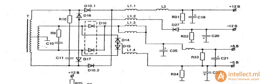
Figure 25 - Diagram of the output rectifier of a typical ATX power supply
Signal conditionersPowerGood
To correctly start the computer's computing system, a power supply delay is organized in the motherboard for a period of time until the transient processes in the power supply are completed and the nominal values of the output voltages are established at the output. For this purpose, a special signal is generated in the power supply PowerGood(“nutrition is normal”). The Power Good signal, delayed by 0.1...0.5 s, represents a logical one level, about +5 V, which is intended for the initial installation of the motherboard.
The formers can be made in discrete and integral versions.

Figure 26 - PG signal conditioner circuit
- LM339; KA339 (four comparators in one housing);
- LM393; KA393 (two in one case) or in the form of a specialized microcircuit M51975A.
Protection and control circuits
Protection of power supplies manifests itself in critical operating modes, as well as in cases where feedback can lead to extreme operating conditions of circuit elements, thereby preventing failure of power and expensive circuit elements.
As a result of the action of the protection circuits, the output control signals are removed from the PWM controller, the transistors of the converter are in the off state, and there is no secondary output voltage. The following protection circuits should be distinguished:
- from short circuit in the load;
- from excessive current in the transistors of the half-bridge converter;
- overvoltage protection.
The first two types of protection are similar in effect and are associated with preventing the converter from delivering high power to the load. They operate when the power supply is overloaded or there is a malfunction in the converter. Overvoltage protection may occur during input voltage surges and in some other cases.
The converter in power supplies is turned off using an additional error amplifier, usually error amplifier 2, turned on by the comparator or via the pause control channel. Below is a description of the protection circuits for the power supplies in question.

Figure 27 - Diagram of protection and control circuits

Figure 28 - Block diagram of a ms PWM controller