Generator circuit for k155la3 with quartz stabilization. Application of digital chips
Electrical processes in transistor multivibrators, operational amplifiers, and logic elements are similar. Structurally, they are also built according to the following circuits: 2 transistors according to the OE or 2LE circuit with the negation of the NAND, NOR, NOR types connected in series. The multivibrator has two temporarily stable states: one LE (microcircuit) is closed, the other is open, and vice versa. Timing parameters R.C.-circuits determine the frequency of the multivibrator.
To build multivibrators using potential logic elements (PLEs), OR-NOT and NAND elements can be used. For multi-input elements, unused inputs are combined, however, the input capacitance increases and the input resistance decreases, or they are connected for the AND-NOT element to + E PIT, for the NOR element to the common bus.
Schematic diagram multivibrator based on AND-NOT elements is shown in Fig. 16.19. The pulse and pause formation times are determined by the capacitor charging time constants R 1 C 1 and R 2 C 2, the discharge occurs through accelerating diodes VD 1 and VD 2 .
Rice. 16.19. Schematic diagram of a multivibrator based on PLE “AND-NOT”
C 1 is charged when the element DD 2 is in the logical “1” state, while the element DD 1- in a logical “0” state. At the moment of element switching DD 2 to state “1”, its output voltage U EXIT DD2=3.5V (for K155 series) will be applied to the input DD 1, because at the moment of switching U C1-= 0, while the output voltage of the element DD 2 U EXIT DD1 drops to 0 V. The multivibrator has the first temporarily stable state ( DD 2 in the logical state “1”, DD 1- to “0”). As the capacitor charges C 1 input voltage DD 1 decreases and at a certain point in time reaches a threshold level U POR ( U POR » 1.5V for the K155 series), at which DD 1 switches to the logical “1” state, which accordingly switches the element DD 2 to the logical “0” state. In this case, the circuit transitions to the 2nd temporarily stable state. In this state the capacitor C 1 discharges and the capacitor C 2 charging. 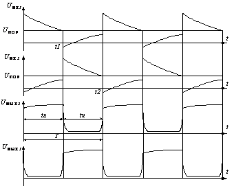
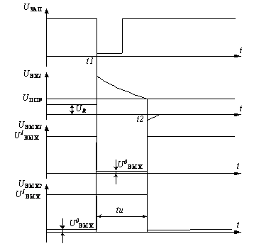
Rice. 16.20. Oscillograms of the operation of a multivibrator on a PLE
Capacitor discharge C 1 through an open diode VD 1 happens quickly, so the moment of the next switch is determined by reaching U VX DD2 =U POR. The circuit again goes into the first temporarily stable state.
DD 1 is closed and U EXIT 1 equal to logical level “1”. This state of the element DD 1 is ensured by connecting a resistor to its input R 1 little resistance. Logic element DD 2 open high level input voltage supplied to one of its inputs. In this case, the capacitor C 1 discharged.
When applied to the input of the circuit at the moment of time t 1 negative impulse trigger element DD 2 goes into a closed state and the voltage at its output reaches the logical level “1”. This positive surge U EXIT 2 transmitted through a capacitor C 1 to element input DD 1, closing it. Voltage U EXIT 1 decreases to the logical level “0”. Capacitor C 1 while charging, the voltage on its plates increases, and U EXIT 1 on a resistor R 1 decreases. At U EXIT 1 =U POR (at t=t 2) the monovibrator flips over, as in a self-oscillating multivibrator. This completes the formation of the pulse and the monovibrator goes into the initial stable state of equilibrium.
The duration of the output pulse and the time the circuit is in a temporarily stable state is determined by the capacitor charging time constant R.C..
Rice. 16.23. Oscillograms of the operation of a single-vibrator on a PLE
This article provides descriptions generators on digital TTL logic chips, such as microcircuits of the K133, K155 and K555 series.
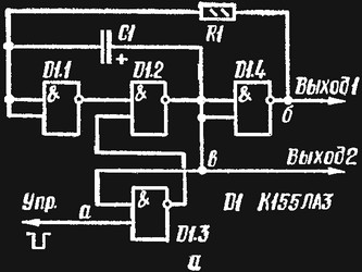
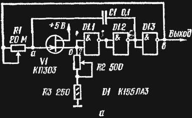
The circuit of one of the simplest generators is shown in Fig. 1, a. The operation of the generator is shown in Fig. 1, b.
Let's agree that the output "Exit 1" element D 1.1 high logical level. At this time, at its input “a” the voltage will be below the switching threshold Up (for K 155 series microcircuits this voltage is approximately 1.15 V), and at the output of element D1.2 "Exit 2"- low logical level.
As capacitor C1 is charged by the output current of element D1.1 flowing through resistor R2 (diode V2 is closed at this time), the voltage at point "V" increases slightly, and at the point "b" decreases. As soon as the voltage at the input of element D1.2 becomes equal to the voltage Up, this element will change its state at its output "G" the logic level will become high.
A voltage surge (from logical 0 to logical 1) through capacitor C2 will go to the input of element D1.1 and switch it to a state with a low logical output level. Capacitor C2 will begin to charge from the output of element D1.2. Capacitor C1 will be discharged by the output current of element D1.1 through diode V2. As soon as the voltage at the input of element D1.1 decreases to the switching threshold, the device will return to its original state and the cycle will repeat.
The duration of the pulses at each of the device outputs is determined by the capacitance of the capacitor.
Rice. 1 Circuit of a simple cross-feedback oscillator (a)
and diagrams of its operation (b) at R1 = R2 and C1 = C2
For stable operation of the multivibrator, it is necessary that the capacitors discharge faster than they charge. This is achieved by turning on diodes V1, V2. With a resistor resistance of 1.8 kOhm and a change in capacitance of the capacitors (C1 = C2) from 100 pF to 0.1 μF, the oscillation frequency of the multivibrator changes from 300 Hz to 2 MHz. When selecting resistors, one must keep in mind that in the absence of oscillations, they must provide a logical level of 1 at the output of elements D1.1 and D1.2 (when the voltage at the inputs of the logical element is zero, the input current is approximately 1 mA). However, if the resistance of the resistors is small, then a significant skew of the top of the generated pulses occurs. Based on this, in a multivibrator based on TTL elements, resistors with a resistance of 100 Ohms to 1.8 kOhms are used (although in most cases the generator operates stably with resistances up to 4 kOhms)
If the capacitances of the capacitors are equal, the duty cycle of the output pulses is 2. By selecting the ratio Cl/C2 with a resistance of resistors Rl and R2 of 1.8 kOhm, you can obtain stable generation with a duty cycle of up to 10 (with a resistance of resistors of 4 kOhm, up to 20).
Inputs "Exercise" serve to control the operation of the multivibrator: generation does not occur when the voltage across them is less than the switching threshold Up (from 0 to 1.15 V). If you do not need to control the operation of the generator, then the inputs "Exercise" it is advisable to connect them through a 1 kOhm resistor to the positive terminal of the power supply (or connect them in parallel to the used input of the logic element, but in this case the input current increases slightly).
To improve the shape of the pulses and eliminate the influence of the multivibrator load, an additional inverter, D1.3, D1.4, should be connected to each output.
In such a device, when the power is turned on, both logic elements can be in the closed state (logical 1 at the outputs), and oscillations will not occur. To prevent this from happening, an additional inverter is also introduced.
Oscillator frequency on digital chips, can be adjusted not only by changing the capacitance and resistance of the timing chains, but also by changing the voltage supplied to the input of the logic elements. In such a generator (Fig. 2), the greater (in absolute value) the control voltage, the greater the generation frequency. When the control voltage changes from 0 to -5 V, the frequency changes according to a law close to linear. When using capacitors C1 and C2 with a capacity of 1000 pF, the frequency adjustment range is 120-750 kHz, and with a capacitance of 0.1 μF - from 1 to 8 kHz.
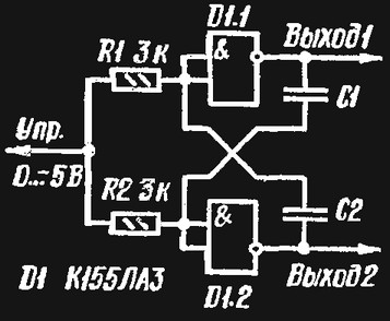
Fig. 2 Diagram of a voltage controlled generator
A simple generator is widely used in practice (Fig. 3, A) , the frequency of the output pulses is determined by the processes of recharging only one capacitor. The principle of its operation is explained by voltage eras (Fig. 3, b). The generator produces pulses in a wide range of frequencies - from a few hertz to several megahertz. Dependence of frequency f (in kHz) on capacitor capacity C1 (in pF) is expressed by the approximate formula f =3*10 5 / C 1. As the supply voltage decreases, the frequency of the generated pulses decreases by approximately 20% for every 0.5 V), and as the temperature increases environment- increases (approximately doubles with an increase in temperature by 100° C).
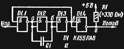
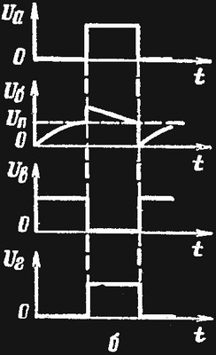
Fig. 3 diagram (a) and voltage diagram (b)
In a generator assembled according to the circuit shown in Fig. 3, a, the logic elements have an open collector. The duty cycle of the pulsed output voltage is almost equal to two.
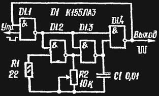
In the generator according to the diagram in Fig. 4, the duration of the pulses can be adjusted by resistor R2 (the duty cycle varies from 1.5 to 3), and the frequency by resistor R1. For example, when using capacitor C1 with a capacity of 0.1 μF in the absence of resistor R2 and changing the resistance of resistor R1 from the maximum value to zero, the frequency of the generated pulses changes from 8 to 125 kHz. To obtain a different frequency range, it is necessary to change the value of capacitor C1.
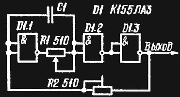
Fig.4 Generator with adjustable pulse frequency and duty cycle
Logic chips allow you to assemble a generator without any other radio components (capacitors, resistors, etc.). The operating principle of such a generator is based on the switching delay of logic elements.
A schematic diagram of one of these generators is shown in Fig. 5, a. When a logical 0 is applied to the control input, the output of element D1.1 will be logical 1 (in Fig. 5, b, the turn-on and turn-off times of the logical elements are assumed to be the same). When logical 1 is applied to the control input, all elements alternately change their state. The third element (D1.3) will switch after a time interval equal to nt bld, where n is the number of logical elements, and t bld is the average switching delay time of one element, equal to half the sum of the on and off delay times. Voltage surge from the generator output through the circuit feedback arrives at the input of element D1.1 and switches it to its original state. Following it, other elements return to their original state.
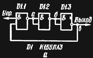
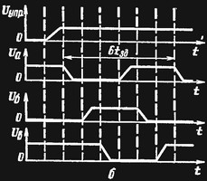
Fig.5 Scheme (a) and generator operation diagram (b)
For K155 series chips, the average latency is about 20 ns. Consequently, a generator assembled according to the circuit in Fig. 5 a, will produce pulses with a repetition frequency of about 8 MHz. If the generator does not start working right away, it is necessary to slightly reduce the supply voltage. To reduce the frequency, the number of logic elements should be increased.
In the examples discussed here, the inputs "Exercise" serve to control the operation of the generator.
Multivibrator, the diagram of which is shown in Fig. 6, a, depending on the period of the input signal, it operates either in standby or in self-oscillating synchronized mode. The multivibrator is triggered by a low logical level or closure, for example by a button, of a control circuit with a common wire.
Rice. 6. Scheme (a) and voltage diagram (b) of a generator operating depending on
duration of control pulses either in the waiting mode (upper diagrams), or in
self-oscillating synchronized (lower diagrams) modes
Elements D1.2 and D1.3 form RS trigger, serving as an electronic key - in the absence of an input signal (which corresponds to applying to the input "Exercise" logical 1), it blocks the operation of the device. If a logical 0 is applied to the control input, the trigger changes its state. In this case, element D1.2 begins to work as an inverter, forming a pulse generator with automatic start with elements D1.1 and D1.4. If the duration of the negative control pulse Ti is greater than the time constant of the circuit R1C1*3, then at least two output pulses are generated with a period approximately equal to 3R1C1. Moreover, the beginning of the first of them coincides with the front of the negative input pulse, and the last pulse, regardless of the moment The end of the enabling signal has the same duration as the previous ones (equal to R1 * C1).
When the duration of the control pulse Ti is less than 3*R1C1, the device generates a pulse (The duration of which is equal to R1C1) for each negative control pulse.
The resistance of resistor R1 can be in the range of 330 Ohm-1.5 kOhm, and the capacitance of capacitor C1 must be at least 50 pF. For example, with a resistor resistance of R = 1 kOhm and capacitor C1 = 100 μF, a pulse with a duration of 100 ms or a sequence of these pulses is generated (depending on the period of the input signal).
Rice. 7. Generator circuit in which the duration of the last generated
pulse does not depend on the end of the control signal
Generator according to the diagram shown in Fig. 7, which generates an integer number of pulse periods at the output, is also triggered by the front of a negative control pulse. Elements D1.2 and D1.3 form an RC generator of rectangular pulses, the repetition frequency of which can be adjusted from 4 to 25 kHz with a variable resistor R2. When a logical 0 is received at the input of element D1.1, an enabling signal is sent from its output to all other elements - logical 1. Therefore, the voltage drop at the output of the device is formed simultaneously (not counting the delay time for switching elements) with the edge of a negative pulse at the control input of element D1. 1. Even if this signal stops (i.e. at the input "Exercise" logical 1) is supplied at a low logical level at the output of the generator, then, thanks to the feedback circuit, logical 1 is maintained at the output of element D1.1, and the device generates the last pulse of full duration. Therefore, the period will always be equal to the previous one.
Typically, the driving circuits of multivibrators include high-capacity capacitors and low-resistance resistors, which limits the range of smooth adjustment of the pulse repetition rate. In the generator, the circuit of which is shown in Fig. 8. a, a similar drawback is eliminated by connecting a transistor switch with a low input current and switching threshold to the input of the microcircuit. The frequency of such a multivibrator can change by a factor of 200(!). Generation occurs when applied to the input "Exercise" logical 1.
![]()
Rice. 8. Scheme (a) and voltage diagrams (b) of a generator whose frequency
variable resistor can be changed 200 times
Let us consider the generation process, starting from the moment the capacitor C1 begins charging (see Fig. 8, b). At this moment, transistor V1 is open and the voltage at its collector is close to zero. At the other input of element D1.1 - logical 1, at the output of element D1.2 - logical 0. Capacitor C1 is charged by the output current of element D1.1 through resistor R1 and the input resistance of transistor V1 and resistors R2, R3 connected in parallel. As capacitor C1 charges, the voltage across it increases exponentially, and the current through it decreases according to the same law. At the same time, the collector current of transistor V1 also decreases, and when it becomes equal to the input switching current of element D1.1, the output of this element will be logical 0, which will switch element D1.2. The negative voltage drop at point a, which closes the transistor at this moment, is formed due to the passage of the pulse front from the output of element D1.1 through capacitor C1.
Next, the capacitor is discharged through resistors Rl - R3 by the output current of the logic elements. When the voltage at point a becomes sufficient to open the transistor, it will open. In this case, the state of element D1.1 will change, capacitor C1 will begin charging, and the cycle will repeat.
Rice. 9. Scheme (a) and voltage diagrams (b) of a generator with a field-effect transistor
The charging time and discharge time of the capacitor, which determine the period and duration of the output pulses, with a static transistor current transfer coefficient of about 100, are determined using the approximate formulas t3 ≈ 3.5*10 -3 C 1, tp ≈ 6*10 -7 (R 2 + R 3)C 1 (capacitance is expressed in picofarads, resistance in ohms, time in microseconds).
When using the elements indicated on the circuit diagram and the total resistance of resistors R2 and R3 20 kOhm, the charging time is about 5.7 μs, and the discharging time is about 18 μs. Resistor R1 allows you to improve the shape of the pulse front. (In principle, this resistor may not exist.)
The multivibrator is capable of generating pulses with both low (less than 2) and large (more than 100) duty cycle. When the capacitance of capacitor C1 changes from 20 pF to 10 μF, the output oscillation frequency changes from 3 MHz to fractions of a hertz.
The frequency of the generator, assembled according to the circuit shown in Fig. 9, a, can be changed by 50 thousand times. This is achieved by using a field-effect transistor. With relatively small capacitor capacities it is possible to obtain ultra-low frequencies. For example, when maximum values indicated on the element diagram, the frequency of the generator output pulses is 0.5 Hz.
The operating principle of the device is illustrated in Fig. 9, b. At the moments of time when element D1.3 goes into a state with logical 1 at the output, the negative voltage drop from the output of element D1.2 passes through capacitor C1 and a negative voltage is formed at point a. Then the capacitor begins to be recharged through resistor R1 by the output current of elements D1.2 and D1.3 (the input current of the field-effect transistor can be neglected). A change in gate voltage leads to a corresponding change in voltage at point b. And when this voltage reaches the switching threshold of element D1.1, it changes its state and thereby switches the remaining logical elements of the generator.
Rice. 10. Generator circuit with quartz frequency stabilization
During periods of time when the output of the device is logical 0, capacitor C1 is discharged until the moment when the voltage at point (b) decreases to the switching threshold of element D1.1, which causes sequential switching of the logic elements (returning them to their original state).
The duration of the output pulses is regulated by resistor R2. Resistor a serves to limit the current through the transistor. The frequency of output pulses can be determined using the formula f=1/ 2*R1*C1 In particular, if the capacitance of capacitor C1 = 0.01 μF and the resistance of resistor R1 is 1 MOhm, the pulse frequency is 50 Hz; with a capacitance of 150 pF and a resistance of 120 kOhm - 22.5 kHz. The upper limit of the generator frequency is about 10 MHz. For smooth frequency adjustment, it is advisable that the variable resistor R1 be multi-turn.
As mentioned above, the oscillation frequency of generators on microcircuits changes quite significantly when the supply voltage and ambient temperature change. If high frequency stability is required, quartz resonators are introduced into the generators. An example is a generator assembled according to the circuit in Fig. 10. It generates pulses in the frequency range 0.1-2 MHz (depending on the resonator B1 used). With appropriate quartz, it is possible to generate pulses with a frequency from 1 to 10 MHz. In this case, capacitor C1 must be excluded, the capacitance of capacitor C2 should be 0.01 μF, and the resistance of the resistors should be 470 ohms. The duty cycle of the generated pulses is about 2.
In such a device, resistors R1 and R2 provide stable generation mode, and element D1.3 serves as a buffer cascade. Capacitor C2 provides decoupling DC. Capacitor C1 prevents high-frequency oscillations at the edges and falls of pulses caused by higher harmonics.
S. Mindelevich
Functional generators are commonly called generators capable of producing several types of signals at once, for example, rectangular, triangular and sinusoidal. The variety of signal shapes of such generators allows them to be used for testing, debugging and researching a wide variety of electronic equipment.
Structural function generator circuit shown in Fig. 161. It works as follows: constant pressure from the output of the Schmitt trigger it goes to an integrator, at the output of which a linearly varying voltage is formed (depending on the state of the trigger, the voltage increases or decreases). The trigger has two response thresholds - upper and lower. Upon reaching one from In them, the Schmitt trigger is triggered, the voltage at its output (and therefore at the input of the integrator) changes, and the formation of the second branch of the triangular voltage begins. The amplitude of the triangular voltage is determined by the difference threshold voltages trigger, and the frequency - the time constant of the integrator and the values of the threshold voltages of the trigger (the smaller the difference in the threshold voltages, the faster the trigger will switch). If it is necessary to generate a sawtooth (asymmetrical triangular) voltage, then it is necessary to automatically change the integration time constant when the sign of the derivative of the triangular voltage changes.
The circuit of the function generator is significantly simplified if the integrator, trigger and sinusoidal voltage generator are implemented on operational amplifiers. At the same time, the number of radioelements decreases, increasing
Rice. 161. Structural scheme function generator
repeatability decreases and the volume of adjustments decreases. In simple generators, instead of conventional op-amps, CMOS inverters can be used. It is known that if an inverter is switched to active mode with the help of external elements, it turns into an inverting amplifier with a transmission coefficient from several tens to several hundreds.
To build a function generator, one K176LA7 microcircuit or similar is sufficient. An integrator is performed on one 2I-NOT element (the inputs are combined and it is turned into an inverter), a Schmitt trigger is performed on two elements connected in series, and another fourth element is used in the sinusoidal signal generation block.
A schematic diagram of one of the variants of a simple function generator is shown in Fig. 162. The Schmitt trigger is made according to the traditional circuit using inverters DD1.2 and DD1.3. Inverter DD1.1 is used in the integrator, and DD1.4 is used in the sinusoidal voltage generator.
For getting best shape sinusoid, the triangular voltage must be strictly symmetrical, therefore, when working with a sinusoidal signal,
Rice. 162, Circuit diagram of a simple function generator
it is necessary to adjust its shape not only with the variable resistor R6 “Form”, which regulates the gain of the op-amp on the element DD1.4, but also with the potentiometer R5 “Symmetry”. The harmonic coefficient of the sinusoidal voltage at the output of the DD1.4 element is large - up to 10% or even more, therefore, for the final formation of the sinusoid, a single-stage low-pass filter R12C4 with a cutoff frequency of approximately 1.4 kHz is included after DD1.4.
At each of the three outputs of the function generator, voltage dividers are installed, with the help of which the amplitudes of rectangular, triangular and sinusoidal signals are equalized. To ensure that the output resistance of the generator is the same across all three outputs, the resistance of the lower arm of the dividers in the circuit is chosen to be the same, equal to 12 kOhm. The output impedance of the generator is quite high - about 10 kOhm, so it is desirable that the input impedance of the devices being tested is at least 100 kOhm, in otherwise the amplitude of the output signal will depend on the value of the input resistance. If this is undesirable, the output resistance of the generator can be lowered by proportionally reducing the resistance of the divider resistors. There are no coupling capacitors at the generator outputs, so the output signals are unipolar. When working with devices that do not have coupling capacitors at the input and the constant component of the generator output signal disrupts their normal operation, the capacitors can be connected to the signal wire break.
It should be noted that despite the fact that the frequency of the function generator can be changed within a fairly wide range, this is not advisable. Firstly, to check the basic characteristics of most radio-electronic components, it is enough to study the passage of rectangular and triangular pulses of a fixed frequency, and secondly, in the simplest functional generators, namely the generator in question, when the frequency changes, the duty cycle (symmetry) of the signal simultaneously changes , and when adjusting the symmetry, the frequency changes slightly. As a result, frequency tuning requires manipulation with two knobs, which is inconvenient in itself and, in addition, the tuning range is narrowed, within which the duty cycle (symmetry) of the output signal remains unchanged. It seems most acceptable to work with a function generator tuned to one fixed frequency.
To test a device in the audio frequency range, it is convenient to take a frequency of 1 kHz as a reference or, for example, to test tape recorders of 400 Hz. It is known that for satisfactory transmission of rectangular pulses with a duty cycle of 2 (meander), the path bandwidth must be at least an order of magnitude higher than the frequency following impulses. With a higher duty cycle, an even larger path bandwidth is required. Thus, by the distortion of the shape of rectangular pulses, one can judge the bandwidth of the path being tested and, if necessary, make adjustments. The small overall dimensions, efficiency and simplicity of the function generator allow it to be built directly into equipment - into a tape recorder, amplifier audio frequency, measuring instrument, etc. - and use during control checks.
Functional generator, the diagram of which is shown in Fig. 162, has the following parameters:
Number of output signals......3 (rectangular
ny, "triangular, sinusoidal
Operating frequency, Hz............ 1000±350
Amplitude of square, triangle and sine wave
signals, V............. 0.28
Effective value of sinusoidal signal, V 0.2
Harmonic coefficient of a sinusoidal signal, %. . 2
Duration of the fronts of the rectangular signal, μs. ... 5
Nonlinearity of the triangular signal, % ...... 3
Current, consumption from a 12 V power supply, mA..................................12
If necessary, the function generator can be made multi-band; to do this, it is enough to install a range switch that switches capacitors C2, C4 and S3, the capacitance of which must be selected for each range.
The functional generator is mounted on a printed circuit board made of single-sided foil fiberglass with a thickness of 1.5... 2 mm. The board for the single-band version of the generator has dimensions of 40X100 mm, its drawing is
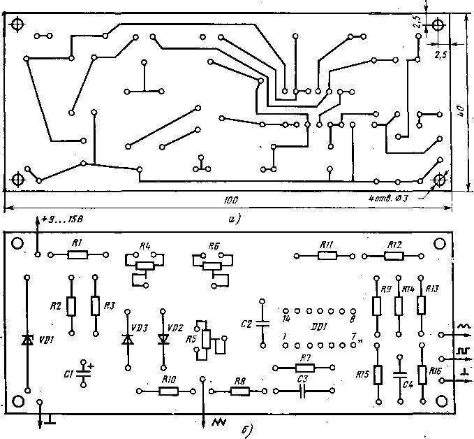
Rice. 163. Board drawing for a single-band version of the generator: a - arrangement of conductors; b - location of parts
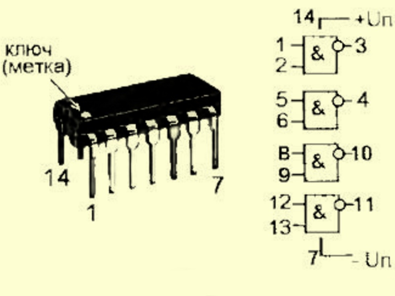
brewed in fig. 163, a, and location of parts -on rice. 163.6. The printed circuit board is designed for the use of MLT resistors with a power of 0.25 W, capacitors KM-6 (C2-C4) and K50-6 (C1), variable resistors SP4-1, diodes KD503B (VD2, VD3), zener diode KS156A (VD1), integrated circuit K176LA7 (DD1).
The circuit is not critical to the parameters and types of radio components used. Resistors and capacitors can be of any type, it is only desirable that capacitor C2 have the minimum possible TKE. Together K176LA7 can be used without changing the pattern printed circuit board microcircuit K176LE5. It is acceptable to use K176PU1, K176PU2, as well as other CMOS microcircuits containing at least four inverters, in particular K561 series microcircuits. In this case, of course, you will have to change the design of the printed circuit board. It is also necessary to take into account the specifics of some series. For example, the K561 series microcircuits can be powered with a stabilized voltage from 3 to 15 V. It should be noted that despite the fact that the rated supply voltage of the K176 series microcircuits is 9 V, most of them operate stably even at undervoltage power supply, which made it possible to power the functional generator with a voltage of 5.6 V. This voltage is not critical and, if necessary (for example, in order to increase the amplitude of the output signal), the supply voltage can be increased by replacing the KS156A zener diode (VD1) with a higher voltage one.
Working with the generator is easy. Different kinds triangular-shaped signals are convenient for checking the linearity of the amplitude characteristics and dynamic range of the device - on straight, with clear bends, the branches of a triangular signal are much better than on a sinusoid, distortions such as “limitation”, “step”, etc. are noticeable. On the fronts of a rectangular signal and On the triangular signal, microexcitations of the device under test are clearly visible, manifesting themselves in the form of emissions.
The sine wave is useful for measuring stage gains, calibrating meters, etc.
One fine day I urgently needed a rectangular pulse generator with the following characteristics:---
Power: 5-12v
---
Frequency: 5Hz-1kHz.
---
Output pulse amplitude is at least 10V
---
Current: about 100mA.
A multivibrator was taken as the basis; it was implemented on three logical elements of a 2I-NOT microcircuit. The principle of which, if desired, can be read on Wikipedia. But the generator itself gives an inverse signal, which prompted me to use an inverter (this is the 4th element). Now the multivibrator gives us positive current pulses. However, the multivibrator does not have the ability to regulate the duty cycle. It is automatically set to 50%. And then it dawned on me to install a standby multivibrator implemented on two of the same elements (5,6), thanks to which it became possible to regulate the duty cycle. Schematic diagram in the figure:
Naturally, the limit specified in my requirements is not critical. It all depends on parameters C4 and R3 - where a resistor can be used to smoothly change the pulse duration. The principle of operation can also be read on Wikipedia. Next: for high load capacity, an emitter follower was installed on the VT-1 transistor. The transistor used is the most common type KT315. resistors R6 serves to limit the output current and is protected from burnout of the transistor in the event of a short circuit.
Microcircuits can be used both TTL and CMOS. If TTL is used, resistance R3 is no more than 2k. because: the input impedance of this series is approximately 2k. I personally used CMOS K561LA7 (aka CD4011) - two housings powered up to 15V.

An excellent option for use as a 3G for any converter. To use a generator among TTLs, K155LA3, K155LA8 are suitable; the latter’s collectors are open and resistors with a nominal value of 1k must be hung at the output.

If the circuit is assembled correctly, the generator starts immediately. The circuit is so simple that even an illiterate schoolchild can repeat it without delving into the principle of operation of the circuit. Good luck... Author of the scheme: comrade bvz.
Discuss the article RECTANGULAR PULSE GENERATOR
In amateur radio practice, there is often a need to configure various converter units of circuits, especially when it comes to inventive activity, when a circuit originates in the head. At such moments, a source of control signal will come in handy.
I present to your attention square wave generator.
Characteristics
Power: 10 ÷ 15 V DC.
Three generation modes:
1 – symmetrical (meander), discrete switching of generated frequency ranges, smooth adjustment frequencies within the range;
2 – independent, discrete switching of generated frequency ranges, smooth separate adjustment of pulse duration and pause between pulses within the range;
3 – pulse width modulation(PWM), discrete frequency selection with a range switch, smooth adjustment of the pulse duty cycle.
Two separate channels - direct and inverse.
Separate adjustment of the output signal level of the channels from 0 V to the value of the power source voltage when connecting a high-resistance load, and up to half the power source voltage when connecting a load with an input resistance of 50 Ohms.
The output impedance of the channel is approximately 50 Ohms.
Basic circuits
To build the generator, we took as a basis oscillator circuit on two logical inverters (Figure 1). The principle of its operation is based on periodic recharging of the capacitor. The moment of switching the state of the circuit is determined by the degree of charge of capacitor C1. The recharging process occurs through resistor R1. The larger the capacitance C1 and the resistance R1, the longer the process of charging the capacitor takes place, and the longer the duration of the switching periods of the circuit state. And vice versa.
To construct the generator circuit, we took as logical elements microcircuit with four 2I-NOT elements – HEF4011BP. The basic circuit shown above allows the output to be Q square wave fixed frequency and duty cycle 50% (meander). To expand the capabilities of the device, it was decided to combine three different circuits in it, implemented on the same two logical inverters.
Square wave generator circuit
The square wave generator circuit is shown in Figure 2-a. The timing capacitance of the circuit can vary from the value of C1 to the total value of C1 and the capacitance connected by jumper P. This allows you to change the frequency range of the generated signal.
Resistor R1 allows you to smoothly change the charge (recharge) current of the capacity. Resistor R2 is current-limiting, to avoid overloading the output channel of logic element DD1.1 in the case when the slider of resistor R2 is in the uppermost position and its resistance is close to zero. Since the charging and recharging of the capacitor is carried out along the same chain with unchanged parameters, the duration of the pulse and the pause between them are equal. Such a signal has a symmetrical rectangular shape and is called a meander. By adjusting R1, only the frequency of the generated signal changes in a certain range specified by the timing capacitor.
Scheme of a rectangular pulse generator with separate adjustment of pulse duration and pause
In Figure 2-b, the charging circuit and the recharging circuit are separated by diodes VD1 and VD2. If a pulse is formed during the charging of a timing capacitor, its duration is characterized by the resistance of the VD1-R2-R1 chain. The duration of the pause between pulses during reverse recharging of the capacity is characterized by the resistance of the circuit R1-R3-VD2. Thus, by changing the position of the sliders of resistors R2 and R3, you can smoothly and separately set the duration of the pulse and the pause between them.
The frequency range of the generated signal, as in the first case, is switched by jumper P.
PWM generator circuit
The circuit in Figure 2-c has a similar separation of the direct and reverse charging circuits of the timing capacitance, with the difference that the variable resistances are the arms of the variable resistor R2, which have an inverse dependence of the parameters in relation to each other. That is, as one arm of the resistor increases, the second one decreases in direct proportion, and the total sum of their resistances is constant. Thus, by adjusting the ratio of the arms of resistor R2, you can smoothly change the ratio of the duration of the pulses to the duration of the pauses between them, and the time of the pulse repetition period will remain unchanged. This adjustment method allows you to implement the pulse width modulation (PWM) function
The frequency of the generated signal in this circuit is selected discretely by switching jumper P. If necessary, you can use several jumpers P to sum large and small capacitance values, achieving a more accurate required signal generation frequency within the entire range.
Final generator circuit
Figure 3 shows generator circuit, in which all three circuits discussed in Figure 2 are implemented. The generator is based on two logical inverters based on elements DD1.1 and DD1.2. The selection of the frequency range (frequency in PWM mode) is carried out by switching jumper P.
To assemble the desired version of the generator circuit, pin connectors are introduced, switched by parallel assemblies of jumpers, shown as colored lines. Each jumper color corresponds to its own connection diagram. The jumpers are implemented by connecting pairs of contacts with wires from the connector cable of type FC-10P A. The pin connectors themselves are located in three groups of five pairs for ease of switching. The jumper connector allows you to switch the generation mode.
Elements DD1.3 and DD1.4 act as inverting repeaters and serve to decouple the timing and output circuits of the generator to eliminate their mutual influence. The inverted signal is taken from output DD1.3, and the main signal from output DD1.4.
Resistors R5 and R6 are used to adjust the voltage level of the pulses of the corresponding channels. Transistors VT1 and VT2 are connected in an emitter follower circuit to amplify the signals taken from the sliders of resistors R5 and R6, respectively. Transistors VT3 and VT4 bypass the output circuits of their channels, pulling them to the power supply negative. Their role is important when applying a generator signal to a load with a capacitance present, when a discharge of this capacitance is necessary during a dead pause, as for example when controlling field effect transistors. Diodes VD5 and VD6 separate the base circuits of the shunt transistors from the generator output, eliminating the influence of capacitive load on the operation of these transistors. Resistors R9 and R10 are necessary to match the generator outputs with a load resistance of 50 Ohms, as well as to limit the maximum current of the transistors of the channel output stages.
Diode VD3 protects the circuit from connecting the supply voltage with reverse polarity. The VD4 LED acts as a power indicator. Capacitor C21 partially smoothes out ripple when powered from an unstabilized source.
Features of the scheme
In order to reduce the dimensions of the device, SMD capacitors C1-C20 are used for the timing capacitance. With the smallest capacitance of the capacitor C1=68 pF, the generator generates a signal with a frequency of up to 17÷500 kHz. With intermediate capacitance values of 3.3 nF and 100 nF, the generator generates signals in the frequency ranges 360÷20000 Hz and 6.25÷500 Hz, respectively. With the smallest capacitance C2 = 5.1 μF, a frequency in the range of 0.2-10 Hz is obtained. Thus, using only four capacitors, it is possible to cover the frequency range from 0.2 Hz to 500 kHz. But at the same time, in PWM mode, it will be possible to generate a signal of only four frequency values using one jumper P. Therefore, to improve the characteristics of the generator, it was decided to introduce 20 capacitors of various capacities into the circuit with a uniform distribution of values over intervals. Additional accuracy of setting the frequency in PWM mode can be obtained by using several jumpers identical to P, which will allow you to adjust the frequency by connecting capacitors of smaller values in comparison with the main additional one.
The power supply of the circuit has some limitations. Despite the fairly wide range of the microcircuit supply voltage 3÷15 V, as experience has shown, when the circuit supply voltage is below 9 V, the generator does not start. At 9 V, starting is not stable. Therefore, it is recommended to use a 12÷15 V power supply.
With a supply voltage of 15 V, a load with a resistance of 50 Ohms connected to one channel of the generator and the maximum output signal level, the device consumes no more than 2.5 W of power. In this case, the main share of power is dissipated at the load and the matching output resistor R9 (R10).
It is not recommended to turn on the generator with a short-circuited load, since the output transistor operates in maximum mode. This also applies to testing circuits with bipolar switches that do not have a limiting resistor in the base circuit. In such cases, it is recommended to reduce the output signal level by at least half a turn of the resistor knob, and then add it as necessary.
In my case, to vary the generation frequency ranges, I used the following series of capacitor values:
C1 - 68 pF;
C2 - 100 pF;
C3 - 220 pF;
C4 - 330 pF;
C5 - 680 pF;
C6 - 1 nF;
C7 - 2.2 nF;
C8 - 3.3 nF;
C9 - 9.1 nF;
C10 - 22 nF;
C11 - 33 nF;
C12 - 47 nF;
C13 - 82 nF;
C14 - 100 nF;
C15 - 220 nF;
C16 - 330 nF;
C17 - 510 nF;
C18 - 1 µF;
C19 - 2.4 µF;
C20 - 5.1 µF.
For any reason, you may use denominations different from those indicated. The only limitation is that the minimum capacitance should not be less than 68 pF, otherwise the generator at this capacitance may simply not start, or begin auto-generation in a non-saturable mode, in which the signal shape is not rectangular, but a distorted rectangle tending to a sinusoid.
The values at which the entire range of generated frequencies is covered are highlighted in red.
Photo gallery
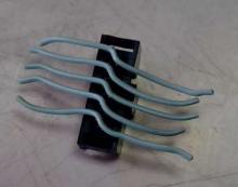
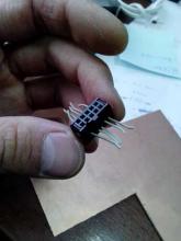
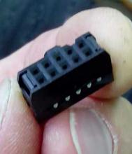
Shown here is the laying of jumper wires in a connector, an assembled connector, and a ready-made jumper connector with cut conductors.
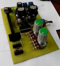
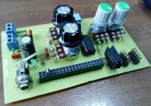
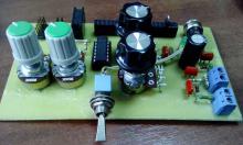
These photos show the generator from different angles
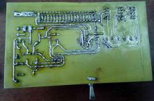
And this is from the signet side. The quality of the tracks turned out to be simply disgusting, which is why we had to make so much tin.
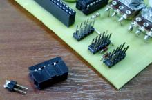
And this, in fact, is a range switching jumper and a mode switching jumper. A little to the right are the sockets and pins that connect these jumpers.
Anyone can make a printed circuit board using parts that are available. Anyone interested in a print of my version of the generator can download the archive from the link below. There is a signet in PDF page format, as well as in PCB format for P-CAD version no lower than 2010. The diagram is also in the archive, you don’t have to try to save it from the page, just download the archive.