Identification of diodes by color marking. Diodes - characteristics, designation and marking of diodes
Semiconductor components
Semiconductor diodes
Classification and designation system for semiconductor diodes
Semiconductor diode called a semiconductor device, usually with one electron-hole junction and two leads.
Semiconductor diodes are divided into groups according to many characteristics. There are diodes made from various semiconductor materials, designed for low or high frequencies, to perform different functions and differ from each other in design.
The designation system for modern semiconductor diodes is established by the industry standard OST 11.336.919-81 and is based on a number of classification characteristics these devices.
The notation system is based on an alphanumeric code.
First element denotes the source semiconductor material from which the device is manufactured.
The following symbols are used to indicate source material:
G and 1 - for germanium or its compounds;
K and 2 - for silicon or its compounds;
A and 3 - for gallium compounds (for example, for gallium arsenide);
And and 4 - for an indium compound (for example, for indium phosphide).
Second element designations - a letter defining a subclass (or group) of devices.
To designate subclasses of devices, one of the following letters is used:
D - rectifier and pulse diodes;
C - rectifying posts and blocks;
B - varicaps;
I - tunnel diodes;
A - ultra-high-frequency diodes;
C - zener diodes;
G - noise generators;
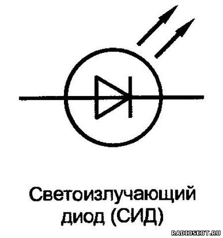
L - emitting optoelectronic devices;
O - optocoupler;
N - diode thyristors;
U - triode thyristors.
Third element designations - a number that defines the main functionality of the device.
To indicate the most characteristic operational characteristics of devices (their functionality), the following numbers are used in relation to various subclasses of devices.
Diodes(subclass D):
1 - for rectifier diodes with a constant or average forward current value of no more than 0.3 A;
2 - for rectifier diodes with a constant or average forward current value of more than 0.3 A, but not more than 10 A;
3- diode converters (magnetic diodes, thermal diodes, etc.);
4 - for pulsed diodes with a reverse resistance recovery time of more than 500 ns;
5 - for pulsed diodes with a recovery time of more than 150 ns, but not more than 500 ns;
6 - for pulsed diodes with recovery time 30... 150 ns;
7 - for pulsed diodes with a recovery time of 5...30 ns;
8 - for pulsed diodes with recovery time 1...5 ns;
9 - for pulsed diodes with an effective lifetime of minority charge carriers less than 1 ns.
Rectifier posts and blocks(subclass C):
1 - for poles with a constant or average direct current value of no more than 0.3 A;
2 - for poles with a constant or average direct current value of no more than 0.3...10 A;
3 - for units with a constant or average forward current value of no more than 0.3 A;
4 - for units with a constant or average forward current value of more than 0.3... 10 A.
Varicaps(subclass B):
1 - for adjusted varicaps;
2 - for multiplying varicaps.
Tunnel diodes(subclass I):
1 - for amplifying tunnel diodes;
2 - for generator tunnel diodes;
3 - for switching tunnel diodes;
4 - for reversed diodes.
Ultra high frequency diodes(subclass A):
1 - for mixing diodes;
2 - for detector diodes;
3 - for amplification diodes;
4 - for parametric diodes;
5 - for switching and limiting diodes;
6 - for multiplying and tuning diodes;
7 - for generator diodes;
8 - for pulse diodes.
Zener diodes(subclass C):
1 - for zener diodes with a power of no more than 0.3 W with a rated stabilization voltage of less than 10 V;
2 - for zener diodes with a power of no more than 0.3 W with a rated stabilization voltage of 10...100 V;
3 - for zener diodes with a power of no more than 0.3 W with a rated stabilization voltage of more than 100 V;
4 - for zener diodes with a power of 0.3...5 W with a rated stabilization voltage of less than 10 V;
5 - for zener diodes with a power of 0.3...5 W with a rated stabilization voltage of 10...100 V;
6 - for zener diodes with a power of 0.3...5 W with a rated stabilization voltage of more than 100 V;
7 - for zener diodes with a power of 5...10 W with a rated stabilization voltage of less than 10 V;
8 - for zener diodes with a power of 5... 10 W with a rated stabilization voltage of 10... 100 V;
9 - for zener diodes with a power of 5...10 W with a rated stabilization voltage of more than 100 V.
Noise generators(subclass G):
1 - for low-frequency noise generators;
2 - for high-frequency noise generators.
Emitting optoelectronic devices(subclass L):
infrared radiation sources:
1 - for emitting diodes;
2 - for radiating modules;
devices for visual presentation of information:
3 - for light-emitting diodes;
4 - for sign indicators;
5 - for sign boards;
6 - for scales;
7 - for screens.
Optocouplers(subclass O):
R - for resistor optocouplers;
D - for diode optocouplers;
U - for thyristor optocouplers;
T - for transistor optocouplers.
Fourth element- a number indicating the serial number of the development of a technological type. To indicate the development serial number, a two-digit number from 01 to 99 is used. If the development serial number exceeds the number 99, then a three-digit number from 101 to 999 is subsequently used.
Fifth Element- a letter that conditionally defines the classification (sorting according to parameters) of devices manufactured using a single technology. Letters of the Russian alphabet are used as classification letters (with the exception of letters 3, O, Ch, Y, Sh, Shch, Yu, Ya, b, b, E).
The following symbols are used as additional designation elements:
numbers 1-9 to indicate modifications of the device leading to changes in its design or electrical parameters;
the letter C to designate assemblies - sets in a common housing of similar devices, not connected or connected by terminals of the same name;
numbers written with a hyphen to designate the following modifications of the design of open-frame devices:
1 - with flexible leads without a crystal holder;
2 - with flexible leads on the crystal holder (substrate);
3 - with rigid leads without a crystal holder (substrate);
4 - with rigid leads on the crystal holder (substrate);
5 - with contact pads without a crystal holder (substrate) and without leads;
6 - with contact pads on a crystal holder without leads, the letter P - after the last element of the designation for devices with paired selection, the letter G - with selection in fours, the letter K - with selection in sixes.
Thus, modern system designations contain a significant amount of information about the properties of the device.
Examples of device designations:
2D921A - silicon pulse diode with an effective lifetime of minority charge carriers less than 1 ns, development number 21, group A;
ZI203G - gallium arsenide tunnel generator diode, development number 3, group G;
AL103B - gallium arsenide emitting diode in the infrared range, development number 3, group B.
Since OST 11.336.919-81 was put into effect in 1982, a different designation system was used for previously developed devices. The symbols for devices developed before 1964 consist of two or three elements.
First element designations - the letter D, which characterizes the entire class of semiconductor diodes.
Second element designation - a number (number) that indicates the scope of application:
from 1 to 100 - for point germanium diodes;
from 101 to 200 - for point silicon diodes;
from 201 to 300 - for planar silicon diodes;
from 301 to 400 - for planar germanium diodes;
from 401 to 500 - for mixing microwave detectors;
from 501 to 600 - for multiplying diodes;
from 601 to 700 - for video detectors;
from 701 to 749 - for parametric germanium diodes;
from 750 to 800 - for parametric silicon diodes;
from 801 to 900 - for zener diodes;
from 901 to 950 - for varicaps;
up to 951 to 1000 - for tunnel diodes;
from 1001 to 1100 - for rectifying posts.
The third element of the designation is a letter indicating the type of groups of similar devices.
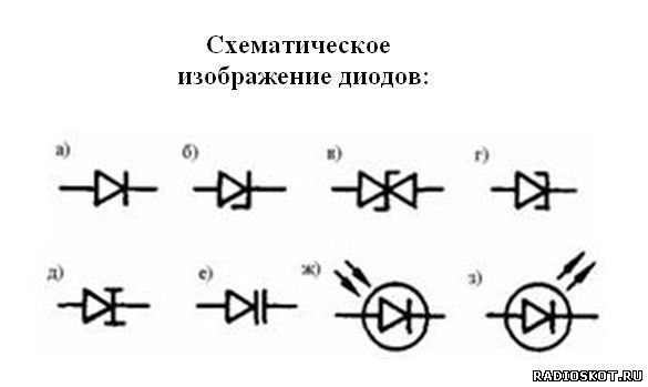
In technical documentation and specialized literature, symbols of semiconductor devices should be used in accordance with GOST 2.730-73.
Graphic symbols of semiconductor devices are given in Table 2.1.
Table 2.1 – Symbols of semiconductor diodes
The reference literature provides the basic standards for semiconductor diodes.
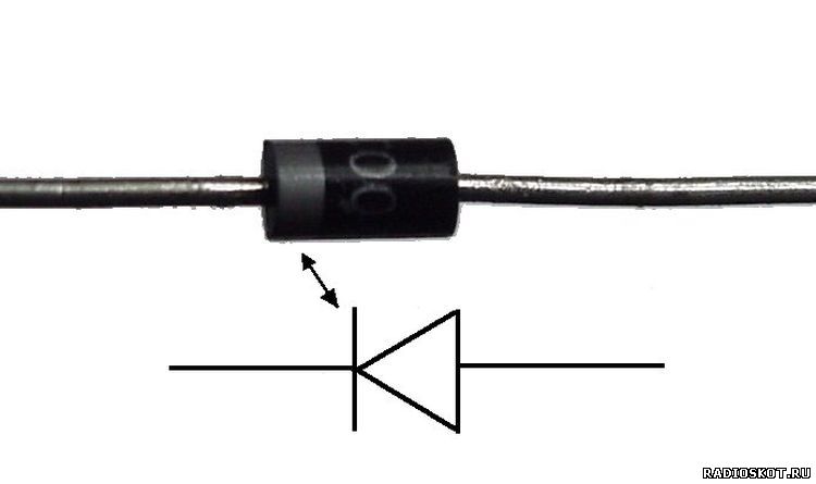
The alphanumeric code of the diodes must be indicated next to their conventional graphic designation (UGO) on the electrical circuit diagrams (Figure 2.1), which describe in detail the elemental base of the electronic device and the electrical connections between electrical radio elements (ERE).
Figure 2.1 – UGO diode with alphanumeric code
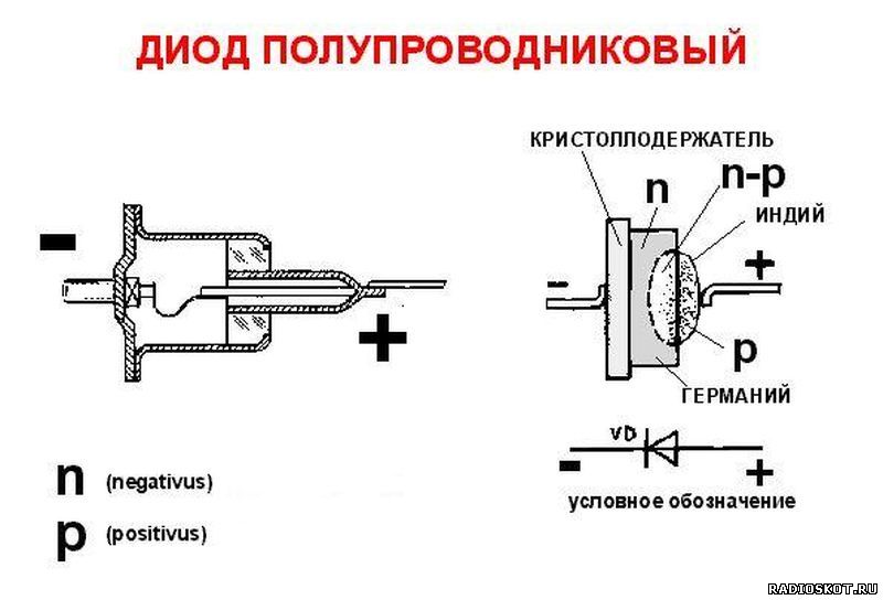
The diode body usually indicates the semiconductor material from which it is made (letter or number), type (letter), purpose or electrical properties of the device (number), letter corresponding to the type of device, date of manufacture, as well as its symbol. The diode symbol indicates how the diode should be connected on device boards.
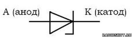
The diode has two terminals, one of which is the cathode (n region), and the other is the anode (p region). In Figure 2.2, the anode is designated by the letter A, and the cathode by the letter K. When connected directly, the anode has a higher potential (plus) and the cathode has a lower potential (minus).
Figure 2.2 – Designation of diode terminals
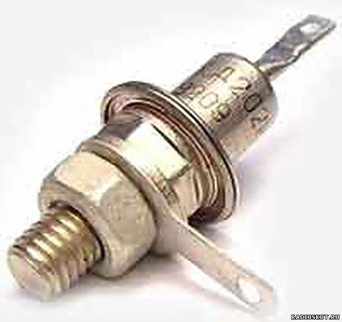
Photographs of different types of diodes are shown in Figure 2.3

Figure 2.3 – Photos of different types of diodes
A conventional graphic image on the body is applied in the form of an arrow indicating the forward direction (Figure 2.4a). If there is no arrow, then a + sign is placed next to the anode. On the flat terminals of some diodes (for example, type D2) the symbol of the diode is directly stamped (Figure 2.4b). When applying a color code, a color mark, dot or strip is applied closer to the anode (Figures 2.4, c, d). Color markings in the form of dots and stripes are given in tables 2.2–2.5. Figure 2.4 also shows the overall dimensions of the diodes in millimeters.
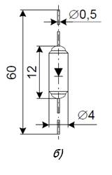

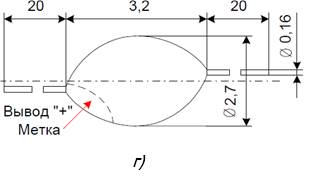
Figure 2.4 – Conventional graphic representation of the diode on the body and color coding in the form of dots
Table 2.2 - Color coding of some types of semiconductor diodes
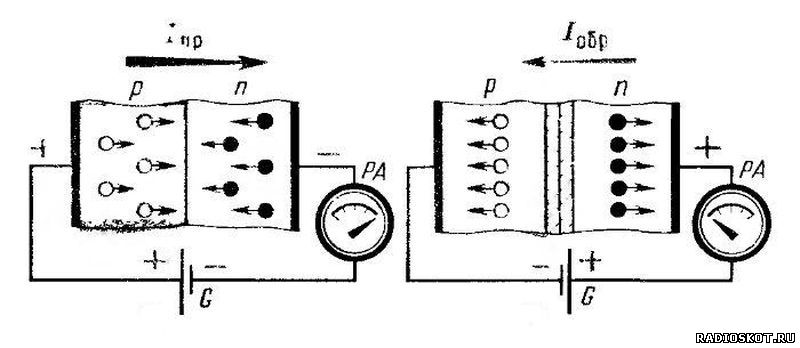
Diode is a two-electrode semiconductor device. This is accordingly Anode(+) or positive electrode and Cathode(-) or negative electrode. It is commonly said that a diode has (p) and (n) regions, they are connected to the diode terminals. Together they form p-n junction. Let's take a closer look at what this p-n junction is. A semiconductor diode is a purified crystal of silicon or germanium, in which an acceptor impurity is introduced into the region (p), and a donor impurity is introduced into the region (n). Ions can act as donor impurities Arsenic, and as an acceptor impurity ions India. The main property of a diode is the ability to pass current only in one direction. Consider the figure below:This figure shows that if the diode is turned on Anode to the plus of nutrition and Cathode to the minus of the power supply, then the diode is in the open state and conducts current, since its resistance is negligible. If the diode is on Anode to minus, and Cathode On the plus side, the resistance of the diode will be very high, and there will be practically no current in the circuit, or rather, it will be, but so small that it can be neglected.
You can find out more by looking at the following graph, Volt-Amp characteristic of the diode:
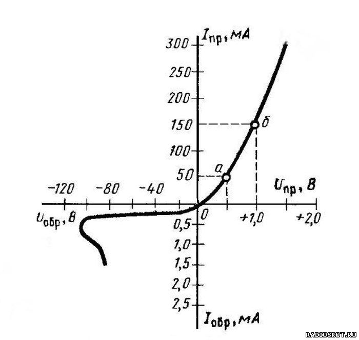
In direct connection, as we see from this graph, the diode has a small resistance, and accordingly passes current well, and in reverse connection, up to a certain voltage value, the diode is closed, has a high resistance and practically does not conduct current. This is easy to verify if you have a diode and a multimeter at hand, you need to put the device in the audio test position, or by setting the multimeter switch opposite the diode icon, as a last resort, you can try to test the diode by setting the switch to the 2 KOhm position for measuring resistance. Featured on circuit diagrams diode as in the figure below, it’s easy to remember where each terminal is: the current, as we know, always flows from plus to minus, so the triangle in the image of the diode seems to show with its vertex the direction of the current, that is, from plus to minus.
By connecting the red probe of the multimeter to the Anode, we can make sure that the diode passes current in the forward direction; on the device screen there will be numbers equal to ~ 800-900 or close to it. By connecting the probes in reverse, the black probe to the anode, the red probe to the cathode, we will see a unit on the screen, which confirms that the diode does not pass current when switched in reverse. The diodes discussed above are either planar or point diodes. Planar diodes are designed for medium and high power and are used mainly in rectifiers. Point diodes are designed for low power and are used in radio detectors; they can operate at high frequencies.
Planar and point diode
What types of diodes are there?
A) The photo shows the diode we discussed above.
B) This picture shows zener diode, (foreign name Zener diode), it is used when the diode is turned back on. Main goal: maintaining voltage stable.
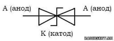
Double-anode zener diode - diagram image
IN) Double sided(or two-anode) zener diode. The advantage of this zener diode is that it can be turned on regardless of the polarity.

D), can be used as a reinforcing element.
D), used in high-frequency detection circuits.

E), used as a variable capacitor.

G), when the device is illuminated, a current arises in the circuit connected to it due to the formation of pairs of electrons and holes.
3), well-known and probably the most widely used devices, after conventional rectifier diodes. They are used in many electronic devices for display and more.
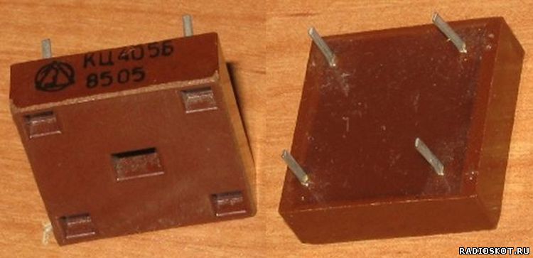
Rectifier diodes They are also produced in the form of diode bridges, let's look at what they are - these are four diodes connected to produce direct (rectified) current in one housing. They are connected by Bridge circuit, standard for rectifiers:
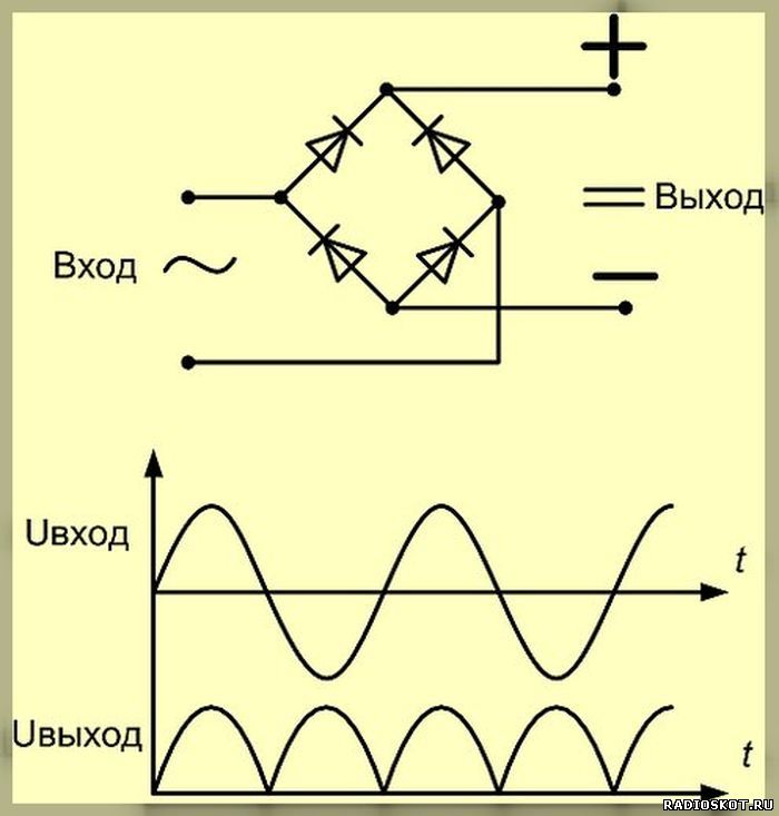
They have four marked pins: two for connection alternating current, and plus and minus. The photo shows a diode bridge KTs405:
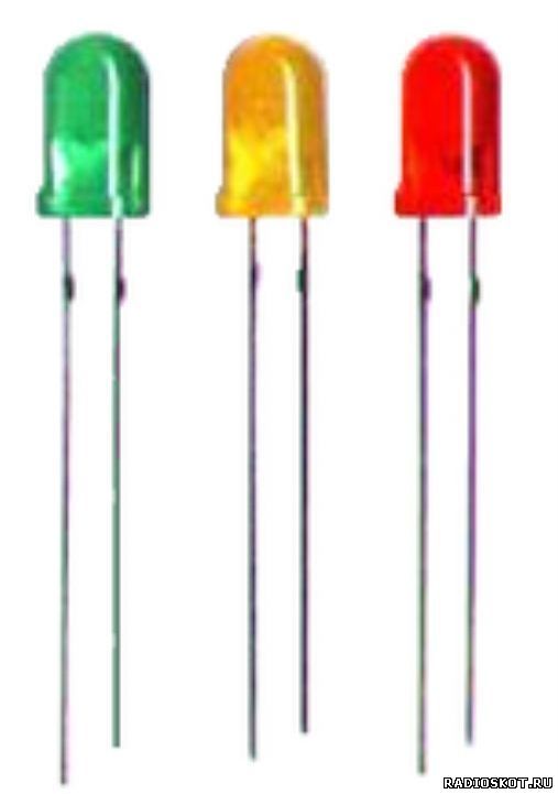
Now let's take a closer look at the area of application of LEDs. LEDs (or rather LED lamp) are produced by industry and for indoor lighting, as an economical and durable light source, with a base that allows them to be screwed into a regular incandescent lamp socket.

LED lamp photo
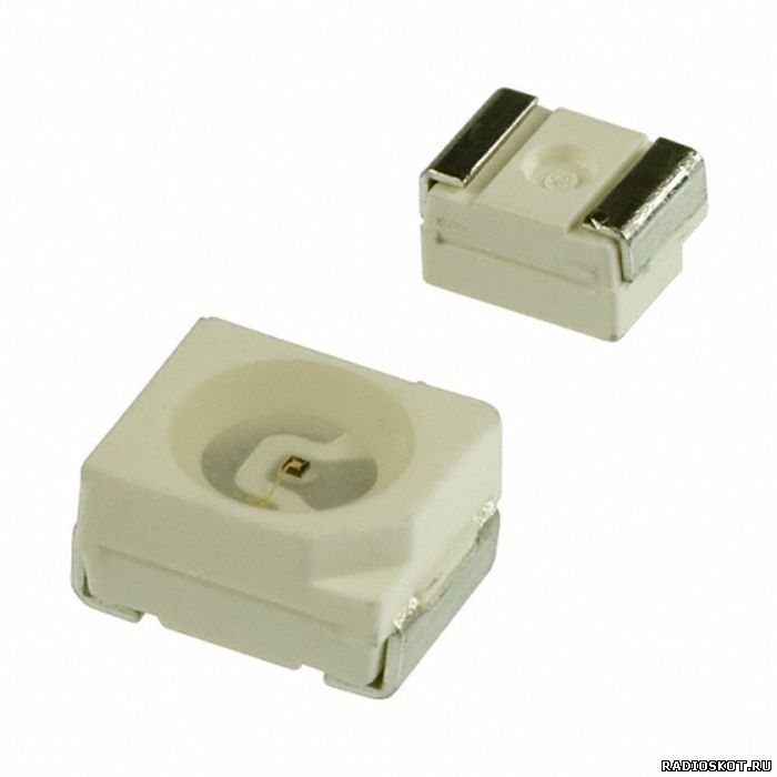
LEDs come in different packages, including SMD.
So-called RGB LEDs are also produced, inside them there are three LED crystals with different luminescence Red-Green-Blue, respectively Red - Green - Blue, these LEDs have four outputs and allow you to get any color visible by mixing colors.

These SMD LEDs often come in strip form with resistors already installed and allow them to be connected directly to a 12-volt power source. You can use a special controller to create lighting effects:

rgb controller
When used, they do not like it when they are supplied with a supply voltage higher than that for which they are designed and can burn out immediately or after some time, so the voltage of the power source must be calculated using formulas. For Soviet LEDs of the AL-307 type, the supply voltage should be approximately 2 volts, for imported ones 2-2.5 volts, naturally with current limitation. For food LED strips, if a special controller is not used, stabilized power is required. Material prepared - AKV.
Discuss the article DIODES
Classification of modern semiconductor diodes(CC) according to their purpose, physical properties, main electrical parameters, design and technological characteristics, the original semiconductor material is reflected in the diode symbol system.
The PD designation system is established as an industry standard OST 11336.919-81, and power semiconductor devices - GOST 20859.1-89. The notation system is based on an alphanumeric code.
The first element (number or letter) designates the source semiconductor material, the second (letter) - a subclass of devices, the third (number) - the main functionality of the device, the fourth - a number indicating the serial number of the development, the fifth element - a letter that conditionally determines the classification (sorting according to parameters) of devices manufactured using the same technology.
The following symbols are used to indicate the source semiconductor material:
- G, or 1, - germanium or its compounds;
- K, or 2, - silicon or its compounds;
- A, or 3, are gallium compounds;
- And, or 4, are indium compounds.
To designate subclasses of diodes, one of the following letters is used:
- D - rectifier and pulse diodes;
- C - rectifying posts and blocks;
B - varicaps;
- I - tunnel diodes;
- A - ultra-high-frequency diodes;
- C - zener diodes;
- G - noise generators;
- L - emitting optoelectronic devices;
O - optocouplers.
To indicate the most characteristic operational characteristics of devices (their functionality), the following numbers are used.
Diodes (subclass D):
1 - rectifier diodes with a constant or average direct value of no more than 0.3 A;
2 - rectifier diodes with a constant or average direct value of more than 0.3 A, but not more than 10 A;
4 - pulse diodes c reverse resistance recovery time of more than 500 ns;
5 - pulse diodes c recovery time more than 150 ns, but not more than 500 ns;
6 - pulse diodes c recovery time 30... 150 ns;
7 - pulse diodes c recovery time 5...30 ns;
8 - pulse diodes c recovery time 1...5 ns;
9 - pulse diodes c The effective lifetime of minority charge carriers is less than 1 ns.
Rectifier posts and blocks (subclass C):
1 - poles with a constant or average direct current value of no more than 0.3 A;
2 - poles with a constant or average direct current value of 0.3...10 A;
3 - blocks with a constant or average current value of no more than 0.3 A;
4 - blocks with a constant or average forward current value of 0.3... 10 A.
Varicaps (subclass B):
1 — adjusting varicaps;
2 - multiplying varicaps.
Tunnel diodes (subclass I):
— amplifying tunnel diodes;
— generator tunnel diodes;
— switching tunnel diodes;
- reversed diodes.
Ultra-high frequency diodes (subclass A):
— mixing diodes;
— detector diodes;
- amplification diodes;
— parametric diodes;
- switching and limiting diodes;
— multiplying and tuning diodes;
— generator diodes;
- pulse diodes.
Zener diodes (subclass C):
1 - zener diodes with a power of no more than 0.3 W with a nominal stabilization of less than 10 V;
2 - zener diodes with a power of no more than 0.3 W with a nominal stabilization of 10...100 V;
3 - zener diodes with a power of no more than 0.3 W with a rated stabilization voltage of more than 100 V,
4 - zener diodes with a power of 0.3...5 W with a rated stabilization voltage of less than 10 V;
5 - zener diodes with a power of 0.3...5 W with a rated stabilization voltage of 10...100 V;
6 - zener diodes with a power of 0.3...5 W with a rated stabilization voltage of more than 100 V;
7 - zener diodes with a power of 5... 10 W with a rated stabilization voltage of less than 10 V;
8 - zener diodes with a power of 5... 10 W with a rated stabilization voltage of 10... 100 V;
9 - zener diodes with a power of 5... 10 W with a rated stabilization voltage of more than 100 V.
Noise generators (subclass G):
— low-frequency noise generators;
— high-frequency noise generators.
To indicate the development serial number, a two-digit number from 01 to 99 is used. If the development serial number exceeds the number 99, then a three-digit number from 101 to 999 is subsequently used.
Letters of the Russian alphabet are used as a qualification letter (with the exception of letters 3, O, Ch, Y, Sh, Shch, Yu, Ya, b, b, E).
The following symbols are used as additional designation elements:
- numbers 1...9- to indicate modifications of the device that lead to changes in its design or electrical parameters;
- letter C- to designate assemblies - sets in a common housing of similar devices that are not electrically connected or connected by terminals of the same name;
- numbers written with a hyphen — to designate the following modifications of the design of open-frame devices:
1 - with flexible leads without a crystal holder;
2 - with flexible leads on the crystal holder (substrate);
3 - with rigid leads without a crystal holder (substrate);
4 - with rigid leads on the crystal holder (substrate);
5 - with contact pads without a crystal holder (substrate) and without leads;
6 - with contact pads on the crystal holder without leads, the letter P after the last element of the designation is for devices with paired selection, the letter G - with selection in fours, the letter K - with selection in sixes.
(PICTURE)
Examples of device designations:
2D204V- silicon rectifier diode with a constant and average current value of 0.3...10 A, development number 04, group B.
KS620A— silicon zener diode with a power of 0.5...5 W, with a rated stabilization voltage of more than 100 V, development number 20, group A.
ZI309ZH— gallium arsenide switching tunnel diode, development number 09, group Zh.
Before introduction in 1982 OST 11336.919-81 a different system of symbols was used. It included two or three elements ( GOST 5461 - 59).
First element- the letter D, characterizing the entire class of semiconductor diodes.
Second element— number (number) defining the scope of application:
1...100 - for point germanium diodes;
101...200 - for point silicon diodes;
201...300 - for planar silicon diodes;
301...400 - for planar germanium diodes;
401...500 - for mixing microwave detectors;
501...600 - for multiplying diodes;
601...700 - for video detectors;
701...749 - for parametric germanium diodes;
750...800 - for parametric silicon diodes.
A diode usually refers to vacuum or semiconductor devices that pass alternating electric current in only one direction and have two contacts for inclusion in an electrical circuit. One-way conductivity of a diode is its main property. This property determines the purpose of the diode:
- conversion of high-frequency modulated oscillations into currents audio frequency(detection);
- rectification of alternating current into direct current.
Detection also means signal detection.
Classification of diodes
Based on the source semiconductor material, diodes are divided into four groups:
- germanium,
- silicon,
- from gallium arsenide,
- from indium phosphide.
Germanium diodes are widely used in transistor receivers, as they have a higher transmission coefficient than silicon.
This is due to their greater conductivity at a low voltage (about 0.1...0.2 V) of the high-frequency signal at the detector input and a relatively low load resistance (5...30 kOhm).
According to design and technological characteristics diodes are distinguished:
- point,
- planar.
By purpose semiconductor diodes are divided into the following main groups:
- rectifying,
- universal,
- impulse,
- varicaps,
- Zener diodes (reference diodes),
- stabilizers,
- tunnel diodes,
- reverse diodes,
- avalanche-span (ALD),
- thyristors,
- photodiodes, s
- LEDs and optocouplers.
Diodes are characterized by such main electrical parameters:
- current passing through the diode in the forward direction (direct current Ipr);
- current passing through the diode in the opposite direction (reverse current Irev);
- the highest permissible rectified CURRENT Ivypr.max;
- the highest permissible direct current Ipr.add.;
- direct voltage Unp;
- reverse voltage iobR;
- highest permissible reverse voltage iobr.max
- capacitance CD between the diode terminals;
- dimensions and operating temperature range.
Old notation system
In accordance with the notation system developed before 1964, the abbreviated designation for diodes consisted of with two or three elements.
First element letter, D - diode.
Second element- number corresponding to the type of diode: 1...100 - point germanium, 101...200 - point silicon, 201...300 - planar silicon, 801...900 - zener diodes, 901...950 - varicaps, 1001...1100 - rectifying columns. Third element- a letter indicating the type of device. This element may be missing if there are no diode varieties.
Currently There is a notation system corresponding to GOST 10862-72. In the new, as in the old system, the following division into groups according to the maximum (limiting) frequency of amplification (current transmission) is accepted into:
- low-frequency LF (up to 3 MHz),
- midrange frequency (from 3 to 30 MHz),
- high frequency HF (over 30 MHz),
- ultra-high frequency microwaves;
By power dissipation:
- low-power (up to 0.3 W),
- average power (from 0.3 to 1.5 W),
- high (over 1.5 W) power.
New notation system
New diode marking system more perfect. It consists of four elements.
First element(letter or number) indicates the source semiconductor material from which the diode is made: G or 1 - germanium* K or 2 — silicon, A or 3 - gallium arsenide , And or 4 - indium phosphide.
Second element- a letter indicating the class or group of the diode.
Third element- a number that determines the purpose or electrical properties of the diode.
Fourth element indicates the serial number of the technological development of the diode and is designated from A to Z.
For example:
- diode KD202A stands for: K - material, silicon, D - rectifier diode, 202 - purpose and development number, A - variety;
- 2C920 - high power silicon zener diode of type A variety;
- AI301B is a gallium arsenide tunnel diode of the switching type B.
Sometimes there are diodes designated according to outdated systems: DG-Ts21, D7A, D226B, D18. D7 diodes differ from DG-Ts diodes in their all-metal housing design, as a result of which they operate more reliably in a humid atmosphere.
Germanium diodes of the DG-Ts21...DG-Ts27 type and diodes D7A...D7Zh, which are similar in characteristics, are usually used in rectifiers to power radio equipment from an alternating current network.
The diode designation does not always include some technical data, so you need to look for them in reference books on semiconductor devices.
One of the exceptions is the designation for some diodes with the letters KS or a number instead of K (for example, 2C) - silicon zener diodes and stabilistors.
After these designations there are three digits, if these are the first digits: 1 or 4, then taking the last two digits and dividing them by 10 we get the stabilization voltage Ust.
For example:
- KS107A - stabistor, Ust = 0.7 V,
- 2S133A - zener diode, Ust = 3.3 V.
If the first digit is 2 or 5, then the last two digits show Ust, for example:
- KS 213B - Ust = 13 V,
- 2C 291A - Ust = 91 V.
If the number is 6, then you need to add 100 V to the last two digits, for example: KS 680A - Ust = 180 V.
Diode marking
The diode body usually indicates the semiconductor material from which it is made (letter or number), type (letter), purpose or electrical properties of the device (number), the letter corresponding to the type of device, and the date of manufacture, as well as its symbol.
The diode symbol (anode and cathode) indicates how the diode should be connected on device boards. The diode has two terminals, one of which is the cathode (minus), and the other is the anode (plus).
A conventional graphic image on the diode body is applied in the form of an arrow indicating the forward direction; if there is no arrow, then a “+” sign is placed.
The flat terminals of some diodes (for example, the D2 series) are directly stamped with the symbol of the diode and its type. When applying a color code, a color mark, dot or stripe is applied closer to the anode (Fig. 1).
For some types of diodes, color markings in the form of dots and stripes are used (Table 1). Old types of diodes, in particular point diodes, were produced in glass and were marked with the letter “D” with the addition of a number and a letter indicating the subtype of the device. Germanium-indium planar diodes were designated “D7”.
Rice. 1. Applying a color code to the diodes.
Table 1 Color coding of semiconductor diodes.
| Diode type |
Ring color (k), dots (t) |
|
| from the cathode side (in the middle of the body) | from the anode side | |
|
Orange t Blue t. Green t. Black t. Red t. |
||
|
Red t. Orange t. Yellow t. Blue t. Green and blue etc. Two yellow t. Two white t. Two green t. |
Red t. | |
|
Yellow t. Orange t. |
Green t. |
|
|
Yellow t. |
||
| White or yellow stripe at the end of the case |
Green t. Red t. White or yellow etc. |
|
| Black, green or yellow mark |
Black t. Green t. |
|
* Body color is brown.
| Diode type |
Ring color (k), dots (t) |
|
| from the cathode side (in the middle of the body) | from the anode side | |
|
Orange k. Red k. Green k. Yellow k. Blue k. |
||
|
KD243Zh |
Violet k. Orange k. Red k. Green k. Yellow k. Blue k. |
|
| KD510A | One wide and two narrow green ones. | |
| 2D510A | One wide and one narrow green k. | |
| KD521A | 1 wide + 2 narrow | |
| KD521B | Blue stripes | |
| KD521V | Yellow stripes | |
| KD522A | One narrow black k. | One wide |
| KD522B | Two narrow black k. | Black ring |
| KD522V | Three narrow black k. | + diode type |
Literature: V.M. Pestrikov. Encyclopedia of amateur radio.
Zener diode
A diode designed to operate in electrical breakdown mode. Conditional
The graphic designation of the zener diode is shown in Fig. 2.5, a.
Rice. 2.5. Graphic representation of semiconductor diodes:
a) zener diode; b) Schottky diode; c) varicap; G) tunnel diode;
d) reverse diode
In this mode, with a significant change in the zener diode current, the voltage changes slightly, i.e. the zener diode stabilizes the voltage. The current-voltage characteristic of the D814D silicon zener diode is shown in Fig. 2.6.
Rice. 2.6. Volt-ampere characteristics
silicon zener diode D814D
In zener diodes, tunnel, avalanche, and mixed breakdown can occur, depending on the resistivity of the base.
In zener diodes with a low-resistance base (low-voltage, up to 5.7IN) there is a tunnel breakdown, and in zener diodes with a high-resistance base (high-voltage) there is an avalanche breakdown.
The main parameters of the zener diode are:
1. Ust– stabilization voltage (at a given current in breakdown mode);
2. Ist.min– minimum permissible stabilization current;
3. Ist.max – maximum permissible stabilization current;
4. rst – differential resistance of the zener diode (in the breakdown area),
Quantities Ust, Ist.min And Ist.max It is customary to indicate them as positive.
For an example of using a zener diode, let us turn to the circuit of the so-called parametric voltage stabilizer (Fig. 2.7.). It is easy to see that if the voltageuinputis so large that the zener diode is in breakdown mode, then changes in this voltage practically do not cause a change in voltageuout (when voltage changesuinputonly the current changesi, as well as voltage ).
Rice. 2.7. Parametric voltage stabilizer circuit
Zener diode is a fast-acting device and works well in pulse circuits.
Stabistor
This is a semiconductor diode, the voltage on which, when connected directly (about 0.7 IN) depends little on the current (the direct branch in the corresponding section is almost vertical). The stabistor is designed to stabilize low voltages.
Schottky diode
The Schottky diode does not usep- n-junction, and the rectifying contact is metal-semiconductor. The symbolic graphic designation of a Schottky diode is shown in Fig. 2.5, b.
Under normal conditions, the forward current formed by conduction band electrons moving from the semiconductor to the metal is very small. This is a consequence of the lack of electrons whose energy would allow them to overcome this barrier.
To increase the forward current, it is necessary to “warm up” the electrons in the semiconductor and increase their energy. Such heating can be accomplished using an electric field.
If you connect an external voltage source with a plus to the metal and a minus to the semiconductorn-type, then the potential barrier will decrease and direct current will begin to flow through the junction. With the opposite connection, the potential barrier increases and the current turns out to be very small.
Schottky diodes are very fast devices; they can operate at frequenciesup to tens of gigahertz (1 GHz=1·10 9 Hz). A Schottky diode can have low reverse current and low
forward voltage (at low forward currents) – about 0.5IN, which is less than silicon
The total diode capacitance at the minimum point of the characteristic is 0.8…1.9 pF. It is useful to note that checking the diode with a tester is not allowed. Tunnel diodes can operate at very high frequencies - more than 1 GHz.The presence of a section with a negative differential resistance on the current-voltage characteristic makes it possible to use tunnel diodes as an amplifying element and as the main element of generators.
Currently, tunnel diodes are used precisely in this capacity in the ultrahigh frequency range.
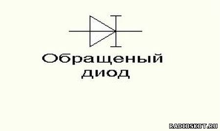
Reversed diode
This is a semiconductor diode, the physical phenomena in which are similar to the physical phenomena in a tunnel diode, so a reverse diode is often considered as a variant of a tunnel diode. In this case, the section with a negative differential resistance on the current-voltage characteristic of the reversed diode is absent or very weakly expressed.
The reverse branch of the I-V characteristic of a reversed diode (characterized by a very small voltage drop) is used as the forward branch of a “conventional diode”, and the forward branch as the reverse branch. Hence the name - reverse diode.
The conventional graphic designation of a reversed diode is shown in Fig. 2.5, d.
Let's take an example current-voltage characteristics germanium reverse diode 1I104A (Fig. 2.9), intended, among other things, for operation in pulsed devices (direct forward current - no more than 0.3 mA, constant reverse current – no more than 4 mA(at ), total capacitance at the minimum point of the current-voltage characteristic 1.2…1.5 pF).
As can be seen from the graph (Fig. 2.9), both branches of the current-voltage characteristic are almost symmetrical (in mirror image) relative to the origin of coordinates. The negative differential resistance section is located on the positive voltage section between 0.1 and 0.3 IN. In this case, the current amplitude in the area with negative differential resistance does not exceed 0.05 mA.
Rice. 2.9. Current-voltage characteristic of a reversed diode.