Big encyclopedia of oil and gas. Topic: “Television broadcast transmitter.” Assignment for a course project.
8. Features of the construction of television systems
The purpose of studying this topic is to familiarize yourself with the basic principles of transmitting a TV signal and audio signal over a radio channel, with the main elements of the structural diagram of a TV system, knowledge of the principles of constructing compatible analogue color television systems, the most important features of color television systems SECAM-3, NTSC, PAL, structural circuits of modern TV receivers.
8.1. Principles of television transmission
In principle, both AM and FM can be used to transmit TV signals over radio channels. In the case of FM, to ensure high noise immunity of transmission, it is necessary that the modulation index m FM be equal to 3-5. In this case, the frequency band f occupied by the frequency-modulated signal will be determined by the relation:
f ![]()
Where ![]() - frequency deviation.
- frequency deviation.
Consequently, to transmit one TV signal you will need a radio channel with a frequency band of about 50-70 MHz. Such an expansion of the radio channel frequency band would lead to a sharp reduction in the total number of transmitted TV signals in the frequency range allocated for TV broadcasting. In a modern TV broadcasting network, only AM is used to transmit TV signals over radio channels, despite the lower noise immunity and worse energy performance of radio transmitters compared to FM. The main advantage of AM is that the amplitude-modulated signal occupies a relatively narrow frequency band.
As is known, AM carrier frequency f leads to the formation of two side frequency bands - lower and upper, each of which is equal to the bandwidth of the modulating signal. If the maximum modulating frequency is f6 MHz, which corresponds to the upper frequency of the TV signal, then the spectrum of modulated frequencies will be equal to ff, i.e. will occupy a band of approximately 12 MHz. Therefore, in order to be able to transmit a modulated TV signal in a standard radio channel having a bandwidth of 8 MHz, the lower side frequency band of the modulated TV signal is partially suppressed, which leads to the elimination of redundancy of information in the amplitude-modulated TV signal.
Figure 8.1. Nominal amplitude-frequency characteristics of radio image and sound transmitters
According to GOST 7845-92, the remainder of the lower side frequency band is 1.25 MHz. In this case, the nominal frequency band of the radio channel allocated for transmitting the TV signal directly is 7.625 MHz (Figure 8.1). Moreover, the attenuation of frequency components - 1.25 and 6.375 MHz relative to the carrier frequency of the image is 20 dB. The 0.75 MHz portion of the lower sideband spectrum is transmitted undistorted. The slope of the lower sideband starting at 0.75 MHz below the image carrier frequency is 40 dB/MHz. In this case, the steepness of the slope of the upper side frequency band, next to which the spectrum of the audio signal is located, is estimated to be more than 50 dB/MHz. With this method of transmitting a TV signal over a radio channel, the amplitude-frequency response (AFC) of the image path of the TV receiver should have the form shown in Figure 8.2. From Figure 8.3 it follows that in TV receivers the level of the image carrier frequency should be attenuated by 6 dB, i.e. 2 times, and the frequency component of 0.75 MHz of the lower sideband should be attenuated by 20 dB, i.e. 10 times compared to the 1.5 MHz reference frequency level in the upper sideband spectrum. If these conditions are met, after detecting a TV radio signal, the total nominal voltage generated at the detector load from the same frequency components of the lower and upper sidebands at any spectral frequency within 0-6 MHz will always be equal to unity if the reading is carried out in relative values. In practice, this means that the shape of the resulting frequency response of the TV radio signal transmission path from the radio transmitter modulator to the TV detector load will be uniform in a given frequency band of 6 MHz.
Figure 8.2. Amplitude-frequency characteristic of the radio path of the TV receiver image
Figure 8.3. Amplifier frequency response intermediate frequency TV receiver images
In each standard radio channel with a width of 8 MHz, in addition to the TV signal, the corresponding audio signal is transmitted (see Figure 8.1). Moreover, the radio audio signal is transmitted using an FM sound carrier frequency, which ensures high noise immunity of the audio path. The maximum frequency deviation is ± 50 kHz with the nominal bandwidth occupied by the radio audio signal not exceeding 0.25 MHz. To use a common antenna-feeder system in radio transmitting devices and a common amplification path to amplify the TV signal and audio signal, it is customary for televisions to transmit the audio signal at a carrier frequency close to the image carrier frequency. In reality, the separation of the audio and video carrier frequencies is 6.5 MHz, and the image carrier frequency is less than the audio carrier frequency. Different types Modulation of TV and audio radio signals greatly facilitates their separation in televisions. In practice, the power of the audio radio transmitter is 10-20% of the power of the TV radio transmitter at the moments of SI transmission. The ratio of the powers of radio image and sound transmitters is selected from the condition of creating identical ranges of action of both transmitters when receiving on standard TV receivers.
Due to the unipolarity of the TV signal, two options for the AM radio signal are possible: negative and positive, depending on the polarity of the modulating TV signal. In most countries of the world, including our country, negative modulation polarity is adopted, in which the maximum level of the image carrier corresponds to the transmission of the SI value, and the maximum value corresponds to the level of the white TV signal. With this modulation polarity, compared to positive, impulse noise appears on the TV image in most cases in the form of dark dots rather than white, so they are visually less noticeable. The noise immunity of the synchronization path of the TV system increases for all types of interference, except pulsed ones, since when transmitting SI TV, the radio transmitter emits the maximum, i.e. peak power. With negative polarity of modulation in TVs, it is easier to carry out automatic gain control (AGC), since in the emitted radio signal, regardless of the content of the TV image, SI corresponds to the maximum and constant value of the emitted power. In addition, the design of radio transmitters is simplified, since the average emitted power is much less than the maximum, since white details are more dominant in TV images. The main disadvantage of negative modulation polarity is the relatively greater influence of impulse noise on the stability of synchronization in TV receivers.
The method of installing the elements of the transmitting TV antenna orients the electric and magnetic vectors of the electromagnetic wave, i.e. determines the plane of polarization of electromagnetic radiation. According to GOST 7845-92, it is allowed to use both horizontal (the electric field vector is located in the horizontal plane) and vertical polarization of waves emitted by a TV radio transmitter. In free space, horizontal and vertical polarizations of electromagnetic waves do not have any advantages over each other. However, in real conditions, especially in cities with a large number of vertically reflecting objects, such as houses, horizontal polarization provides a lower level of reflected interfering waves, which cause signal fading and interference on the TV image in the form of additional contours. In addition, with horizontal polarization, there is less exposure to industrial interference, in particular interference from vehicle ignition systems, which have a vertically polarized component.
![]()
Finally, the designs of TV antennas with narrow radiation patterns for receiving horizontally polarized electromagnetic waves turn out to be simpler and easier to install on metal supports. Therefore, when organizing TV broadcasting in most countries of the world, preference was given to horizontal polarization of electromagnetic radiation.
8.2. Generalized block diagram of a television system
A modern TV system (Figure 8.4) consists of two parts: transmitting and receiving, connected by a communication line. In the transmitting part of the system, the image of the observed object is projected using lens 2 onto the transmitting tube 3, located in the transmitting TV camera 1. The transmitting tube, during the scanning process, generates a video signal, which, after pre-amplification in the amplifier of the TV camera 5, enters TV channel 7. For TV scanning 4 transfer tubes are supplied to the deflection system electrical signals sawtooth shape of horizontal frequency and field frequency. These signals are generated in the scanning unit 6 of the transmitting chamber. In the TV channel, the video signal is further amplified, its distortions are corrected and a complete TV signal is formed, for which blanking and SI lines and fields are mixed into the video signal. These pulses are input into the TV channel from a special pulse generator - synchronizer 9. The synchronizer generates the pulses necessary for the operation of the entire TV system and ensures a strict frequency ratio between them. The SI generated by the synchrogenerator ensures synchronism and in-phase scanning of the receiving and transmitting tubes. Since the scanning unit of the transmitting tube is located directly in the transmitting chamber, the CSI and SSI are separately supplied to the corresponding generators of the scanning unit directly from the clock generator. The mixture of clock pulses required to synchronize the scanning unit of the receiving tube is transmitted along with the video signal.
The generated and amplified full TV signal is supplied to the modulator of the radio transmitter 8, where it modulates its carrier frequency, and then enters the transmitting antenna in the form of high-frequency oscillations.
The radio signals received by the receiving antenna directly enter the TV receiver. Modern TV receivers are built only using a superheterodyne circuit. Televisions use joint amplification of image and audio signals by a high-frequency path, followed by their separation and additional amplification. Depending on the point of signal separation, the amplification path of a TV receiver is built according to one of two options, called single-channel and two-channel.
A single-channel scheme assumes a common amplification at the intermediate frequency of the TV signal and the audio signal (see Figure 8.4). Therefore, in the high-frequency part of the TV 10, the appropriate channel is selected, the radio signals are pre-amplified and their frequency conversion into intermediate frequencies of image (38 MHz) and sound (31.5 MHz). Both signals, after conversion, are amplified by one multistage intermediate frequency amplifier 11, which has a fairly wide bandwidth, and then detected by an amplitude detector 12. The video detector is a nonlinear element and performs the function of a simple converter. Therefore, at its input, in addition to the video spectrum, a beat frequency signal is also generated between the intermediate carrier frequencies of image and sound. The difference signal with a frequency f=38-31.5 MHz is modulated in frequency and amplitude. Helpful information, corresponding to the audio signal, is determined by the FM signal of the difference frequency.
The main advantage of a single-channel TV receiver circuit is not only that there is no need to have separate local oscillators and mixers for image and sound signals, but also that there is no instability in the audio signal tuning associated with changes in the local oscillator frequency in block 10. B in this case deviation of the frequency of the generator of the high-frequency block of the TV from the nominal leads to an equal change in the intermediate frequencies of the video signal and audio signal, and the difference frequency, equal to 6.5 MHz, remains unchanged. The intermediate frequency amplifier, amplitude limiter and frequency detector included in the audio channel 13 are tuned to the difference frequency. In addition, block 13 also includes a low-frequency amplifier, from the output of which an amplified audio frequency signal is supplied to the acoustic system 14.
The full TV signal, amplified by the video amplifier 15, is fed to the color block 16, in which video signals of primary colors are generated and supplied to the color kinescope 17.
From the output of the video amplifier, the signal also enters synchronization channel 18, in which the separation of synchronization pulses from the video signal and the separation of SSI and SSI are ensured. Next, these pulses synchronize the master oscillators of the blocks of frame 19 and line 20 scans of the electron beams of the kinescope, respectively. The deflection currents generated by the scan generators are supplied to the deflection system of the kinescope. In addition, the output stage of the horizontal scan generator simultaneously serves as a source high voltage to power the kinescope, which is obtained by rectifying the horizontal frequency pulses generated in the autotransformer winding of this stage. Modern TV receivers use automatic adjustments of a number of parameters, for example, brightness, raster size. Receiver blocks 10, 11, as a rule, are covered by an AGC circuit, which ensures that the output level of the video signal is maintained both when reception switches from one program to another, and when the conditions of radio wave propagation and other factors affecting the magnitude of the video signal change.
8.3. Broadcast analogue color television systems
Principles of building color television systems. Modern color television is based on the theory of three-component color vision, from which it follows that by mixing the three main spectral colors taken in certain proportions, you can get all possible colors. In this case, the primary colors must be linearly independent, i.e. neither of them can be obtained by mixing the other two. The following colors of monochromatic radiation are usually taken as the main colors: red (R) with a wavelength = 700.1 nm, green (G) = 546.1 nm, blue (B) = 435.8 nm. For example, equal-energy white color can be obtained by mixing the primary colors R, G, B in equal proportions.
For television transmission, the multi-color image of the object on the transmitting side must be divided into three single-color images (in red, green and blue). Next, video signals E, E, E of these single-color images should be transmitted over a communication channel by analogy with black-and-white TV. On the receiving side, to obtain a color image of an object, it is necessary to reproduce three single-color images and combine them.
The most important requirement for color TV systems is compatibility, which means:
- the ability to receive color broadcasts in black and white on existing black and white
TVs (direct compatibility); - reception of black and white TV signals on color TVs (backward compatibility);
- transmission of color and black-and-white TV signals over the same communication channel (in the frequency band of black-and-white TV).
To ensure compatibility in color TV, it is necessary to have a signal that would create a normal black and white image with the correct reproduction of the brightness gradations of a color object. Therefore, in compatible color TV systems from those received at the transmitting end video signals of primary colors E, EE, a luminance signal E is formed
E=0.3E+0.59E+0.11E, (8.1)
in which the numerical values of the coefficients that determine the share of voltages of video signals of primary colors are selected taking into account the characteristics of the adopted reference white color D (source with color temperature 6500K, corresponding to the radiation of the daytime cloudy sky) and the chromaticity coordinates of the phosphors of modern color picture tubes. The brightness signal E, in accordance with expression (8.1), is generated using a coding matrix, which is a resistive voltage divider with a common load.
In addition to the luminance signal, chrominance information must be transmitted in a compatible color TV system. In practice, it is sufficient to transmit only two color signals to the receiving end, for example, E and E. The third color signal E can be easily obtained at the receiving end by matrixing based on equation (8.1). However, direct transmission of signals E and E is impractical, since these signals, in addition to color information, contain redundant information about brightness, which is already present in the E signal. Therefore, in all compatible color TV systems, color difference signals are transmitted
which are formed by subtracting the brightness signal E from E and E. The peculiarity of color difference signals is that they do not contain information about brightness. For example, their amplitude is zero when transmitting white or gray areas of the image, when E = E = E = E, and is small in weakly saturated colors. Since such colors usually predominate, the average amplitude of color difference signals is much less than the maximum and much less than the average amplitude that would be when transmitting signals E R, E G, E. This greatly improves the noise immunity and compatibility of color TV systems. Moreover, it is enough to transmit color difference signals in a reduced bandwidth of up to 1.5 MHz. This is explained by the peculiarities of visual perception of color images. Experimental studies have shown that the human visual apparatus perceives only large and medium-sized image details in color. Small details, which correspond to frequencies of color difference signals greater than 1.5 MHz, can be reproduced in black and white, while overall rating The quality of the color image will hardly deteriorate.
In compatible color TV systems, the luminance and color difference signals must be transmitted in the standard black-and-white TV frequency band. For this purpose, the spectrum of the brightness signal is compressed with chrominance signals.
In practice, one or two subcarrier frequencies modulated by two color difference signals are introduced into the spectrum of the luminance signal. The method of transmitting and receiving color difference signals distinguishes modern color TV broadcasting systems from each other. Currently, three color television broadcast systems are in operation in various countries around the world. For example, in the USA, a color system with quadrature modulation of the subcarrier frequency NTSC (National Television System Committee, i.e., a system proposed by the National Committee of TV Systems) has been developed. The NTSC system is used in 54 countries with a population of 870 million people. In Germany, a system with quadrature modulation and a horizontally variable phase PAL (Phase Alternation Line) has been developed. The PAL system is used in 81 countries with a total population of 3.5 billion people. In our country and in 60 other countries of the world with a population of 760 million people, a color television system with sequential transmission of color-difference signals and frequency modulation of SECAM-III subcarriers is used.
SECAM-III color television system. A distinctive feature of this system is the use of FM to transmit color difference signals. FM is adopted to reduce differential distortion, i.e. dependences of the subcarrier phase (differential phase distortion) and its amplitude (differential gain) on the brightness signal level. Consistent transmission of FM color signals practically frees this system from phase distortions that affect the quality of color rendering. In addition, the SECAM-III system eliminates cross-distortion between chrominance signals and associated color tone distortion, since at each instant along the channel the chrominance signal modulates its subcarrier in frequency. The subcarriers are harmonics of the horizontal frequency and are spaced 10 line intervals apart:
f = 282 f = 4.40625 MHz ± 2 kHz,
f = 272 f, = 4.25 MHz ± 2 kHz,
where f = 15625 Hz – horizontal scanning frequency.
The choice of two subcarrier frequencies made it possible to increase the transmission noise immunity while maintaining system compatibility.
The possibility of alternating (through a line) transmission of color signals is based on the characteristics of the human visual apparatus. Since small image details are perceived in black and white, an increase of approximately 4 times in the size of image details reproduced in color is also permissible in the vertical direction.
To improve compatibility and noise immunity, the frequency modulator of the transmitting device receives slightly modified color-difference signals, which are usually designated by the symbols D and D. These signals are formed from the color-difference signals E and E as follows:
D = -1.9E, D = 1.5E.
The introduction of coefficients for E and E ensures the same maximum frequency deviations. The minus sign in the equation for signal D indicates that this signal is inverted. This is done in order to reduce the visibility of the subcarrier on TV screens when transmitting the most common colors (red, orange, yellow) and avoid limiting the subcarrier in the image transmission path.
The visibility of subcarriers on TV screens is affected by its scope. Therefore, subcarriers are transmitted with compression. In practice, the subcarrier level is chosen to be approximately 20% of the peak-to-peak luminance signal E. For example, Figure 8.5 shows the combined spectra of the SECAM-III system.
Figure 8.5. Combined spectra of SECAM-III system signals
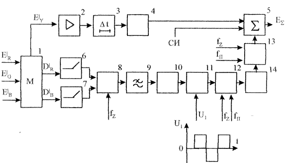
Figure 8.6. Block diagram of the SECAM-III encoder
The formation of all SECAM system signals transmitted over the communication channel is carried out in the encoding device (Figure 8.6). Video signals of primary colors , , , subjected to gamma correction (the prime sign means gamma correction of signals), from the output of the camera channel are supplied to the encoding matrix 1, with the help of which a brightness signal and two color difference signals are generated and in devices 6, 7 the signals are subjected to low-frequency pre-emphasis. Electronic switch 8 provides sequential switching of color difference signals from line to line. Limitation of the frequency spectrum of signals alternating in time is carried out using a low-pass filter 9. Before applying signals to the input of a frequency-modulated generator (FMG) 11, they are subject to amplitude limitation in the amplitude limiter 10. The need for amplitude limitation is explained by the appearance of emissions in color signals that arise at color transitions as a result of low-frequency pre-emphasis. In HMG, subcarriers are generated and modulated, and the signals are modulated by different subcarriers. Therefore, voltage U1 is applied to the HMG, which is symmetrical pulses of half-line frequency, changing the resting frequency of the frequency modulator from line to line. After the FMG, the signal enters the subcarrier phase switching unit 12, which changes the phase of the subcarrier frequencies by 180° at the beginning of every third line and each field. This is done to improve compatibility by reducing the visibility of subcarrier interference on TV screens. The next element of the encoder through which the color signals pass is the high-frequency pre-emphasis circuit 14, which increases the amplitude of the frequency-modulated components generated by the HMG. In the subcarrier suppression block 13, the color channel is turned off at time intervals corresponding to the transmission of synchronization signals for TV receivers. This is necessary to ensure that subcarrier oscillations do not interfere with the synchronization pulses.
The brightness channel of the encoding device includes an amplifier 2, a delay line (DL) 3, a cross-distortion corrector 4. In the summing device 5, the color signals are added to the luminance signal and synchronization pulses for receiving devices. With the help of LZ, the time combination of brightness and color signals is carried out, which arrive at adder 5. The need to turn on LZ is due to the additional delay of signals in pre-emphasis, low-pass filter and HMG devices. The crosstalk corrector is designed to reduce interference in the TV that occurs due to beats between the chrominance signals and the high-frequency components of the luminance signal.
A distinctive feature of the SECAM-III system is the pre-emphasis of color difference signals before their transmission over the communication channel, carried out in the encoding device. To increase noise immunity, the encoder provides a rise in high-frequency components of color-difference signals and = 4.28b MHz.
With the help of this pre-emphasis, the visibility of subcarriers in a black-and-white image when transmitting low-saturated colors is weakened and the noise immunity of color signal transmission is increased. Graphically, the dependence of the transmission coefficient of the high-frequency pre-emphasis circuit is shown in Figure 8.8.
The process of sequential transmission of color signals requires their recognition in receiving devices. For this purpose, color synchronization signals are transmitted in the SECAM-III system with field frequency. The identification signal is generated in the encoding device of the telecentre in the form of a series of 9 trapezoidal pulses of negative polarity, transmitted after the second group of equalizing pulses during the operation of the KGI.
The color burst signal occupies lines 7-15 in odd fields and 320-328 in even fields.
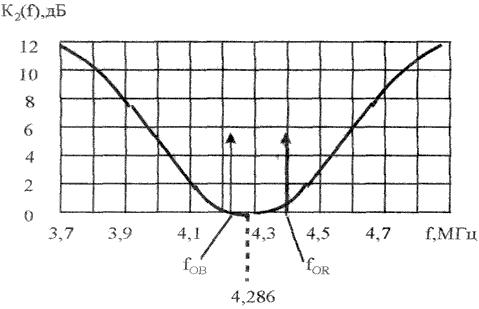
Figure 8.8. Characteristics of the high-frequency pre-emphasis circuit
Moreover, the duration of each trapezoidal pulse corresponds to the time interval of scanning one line of the image. The color recognition signal U op is entered into the coding matrix of the transmitting equipment of the SECAM-III system in both color difference R-Y signal and B-Y before they are converted to and . After converting the color-difference signals together with the E "R-Y signal, the polarity and its identification signal change. Therefore, the trapezoidal pulses in the D" R signal have a positive polarity, and in the B signal - negative (Figure 8.9). At the output of the encoder, the color synchronization signal consists of packets of color subcarriers modulated by trapezoidal-shaped pulses.
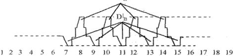
Figure 8.9. Color Burst Waveform
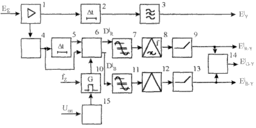
Figure 8.10. Block diagram of the SECAM-III decoding device
In the receiving decoding device (Figure 8.10), the full signal E" Y after the video detector is amplified in amplifier 1 and divided into two channels: brightness and color information. The signal E" Y passes through LZ 2, similar to that in the encoding device, and notch filter 3, suppressing the frequency-modulated chrominance signal in the brightness signal.
In the chrominance channel, the signals D" R, D" B are supplied to the high-frequency pre-emphasis corrector 4, which eliminates the AM subcarrier caused by high-frequency pre-correction in the encoder. Thus, at the output of device 4 there is a sequence of frequency-modulated color difference signals D" R and D" B alternating from line to line.
An important component of the TV decoding device is the color synchronization circuits. It is necessary to ensure that the signals D" R and D" B arrive at their frequency detector. To do this, it is necessary to establish the correct initial phase of operation of the electronic switch. This function is performed by color synchronization circuits, consisting of a control generator of rectangular pulses 10 and an identification unit 15, controlled by the Uop signal.
Based on the fact that TV broadcasting via the SECAM-III system in Russia will continue for many years to come, domestic research organizations are working to improve the quality of the reproduced TV image. For example, a widescreen TV system SECAM plus, compatible with the existing SECAM-III system, has been proposed.
New system provides:
- compatibility with the existing fleet of color TVs;
- improving image quality;
- image format equal to 16:9;
- stereo sound.
Brief information about color television systems NTSC, PAL. In a compatible NTSC system, simultaneous color difference signals are transmitted on a single subcarrier using quadrature modulation. The color subcarrier generator produces highly stable oscillations of frequency f 0, which is the odd harmonic of half the horizontal scanning frequency. With this choice of color subcarrier, a fractional number of carrier periods will fit into the duration interval of one line, i.e. an integer number of periods and a half period. And since with interlaced scanning one frame contains an odd number of lines, the phases of the subcarriers in the same lines of two consecutive frames will be opposite. This results in an average of the visually observable brightness produced in the black and white image of the color subcarrier, thereby reducing its visibility. In practice, the frequency of the color subcarrier in a TV system with the number of decomposition lines Z=625 lines is chosen equal to 4.43 MHz, and in the case of the standard Z=525, f 0 = 3.58 MHz.
To implement quadrature modulation of the color subcarrier, the encoder has two balanced modulators. One of them receives a signal from the subcarrier generator U 0 cosw 0 t and a color difference signal, and the other receives a subcarrier signal Usinwt phase shifted by 90 and a color difference signal. The output voltages of balanced modulators are proportional to the products of the input voltages when suppressing the subcarrier. This eliminates the interfering effect of the color subcarrier on the reproduced image. In the addition block, both color difference signals transmitted on the subcarrier are linearly added, forming the resulting color signal U CV, the magnitude and phase of which are respectively equal:
U CV = ![]() , = arctan (
, = arctan ( ![]() ).
).
From these relationships it is clear that the resulting color signal varies in amplitude and phase. Moreover, the amplitude of the signal characterizes the color saturation, the phase - the color background.
Taking into account the unequal resolution of vision when perceiving small details painted in different colors, in the NTSC system, instead of the signals E 1 R-Y and E 1 B-Y, the following signals E 1 I = 0.74E 1 R-Y - 0.27E 1 B-Y, E are formed using matrixing 1 Q = 0.48E 1 R-Y + 0.41E 1 B-Y .
The transmission of signals E 1 I and E "Q is carried out in different frequency bands. For example, the signal E 1 Q is transmitted in the band ± 0.5 MHz (frequency is measured from the subcarrier value), and the signal E 1 I is transmitted in the band from -1. 4 to +0.5 MHz, i.e. with partial suppression of the upper sideband (Figure 8.11).
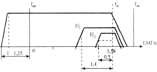
Figure 8.11. Spectrum of NTSC TV signal
On the transmitting side, the resulting chrominance signal Ucolor is mixed with the luminance signal E "Y and then fed to the TV radio transmitter. For proper operation of the TV, it is necessary to restore the frequency and phase of the color subcarrier. For this purpose, as part of the complete TV signal of the NTSC system, a sync flash signal is transmitted in the form 79 periods of the color subcarrier f 0, located on the rear platforms of the SGI.
In TV receivers, synchronous detectors are used to inversely separate the resulting color signal into color difference signals. They are also supplied with oscillations from a local color subcarrier generator with a phase shift of 90° for signals E" I and E" Q. The frequency and phase of oscillation of the subcarrier frequency generator is set under the influence of the sync flash released by the TV selector. Next, from the received signals, color-difference signals E R-Y ", E G-Y 1, E B-Y " are formed by matrixing, which are fed to the modulators of a three-beam color kinescope.
The main disadvantage of the NTSC system is its sensitivity to signal phase distortions that occur in the communication channel and manifest themselves mainly in changes in color tone.
The PAL compatible color TV system, like NTSC, uses quadrature modulation of one subcarrier to transmit color difference signals. This system eliminates color distortions in images by compensating for phase distortions of the signal. To do this, in the PAL system, on the transmitting side, a periodic change in the phase of the subcarrier of one of the color difference signals (E R-Y ") from line to line by 180° is used. In the TV receiver, an LZ is set for the color signal for the duration of the transmission of one line. Moreover, at the output of the delay line, periodic change in the polarity of the color difference signal E R-Y ". The simultaneous presence of two color signals of adjacent lines on the TV allows them to be added, which leads to the elimination of color distortions.
The principle of phase distortion compensation is illustrated in Figure 8.12.
Let, as a result of phase distortions in the transmission path, the quadrature-modulated signal U CV1 1 shift relative to the initial position U CV1 by an angle counterclockwise (see Figure 8.12 a). Then Figure 8.12b shows the resulting chrominance signal U CV2 for the next line and the signal U CV2 1 actually shifted by an angle in the same direction. The addition of color signals should be done according to the rules of vector addition. From Figure 8.12c it is clear that as a result of adding the signals U TsV1 1 and U TsV2 1 the resulting signal U TsV.R is formed, the value of which is approximately equal to twice the value of the original terms, and the direction coincides with the original signal U TsV1, i.e. phase shift compensation occurs. Moreover, the almost doubled swing of the signal U TsV.R due to the limitation is brought to the normal value U TsV1.
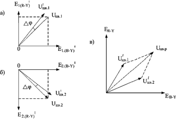
a, b) vector diagrams of two adjacent lines, c) the resulting color signal after the adder
Figure 8.12. Phase distortion compensation circuit in the PAL system
One of the important disadvantages of the PAL system is some complication of the TV receiver due to the introduction of additional devices to delay the color signal for the duration of one line and periodically change the phase of the color difference signal E R-Y ".
8.4. Design features of modern television receivers
Modern stationary televisions are classified into three groups and have the following designations, respectively: 3USCT (unified stationary semiconductor-integrated televisions of the third generation); 4USTST, 5USTST.
A characteristic feature of the 3USCT series televisions was their complete transistorization, as well as the use of large integrated circuits and color picture tubes with self-converging electron beams (planar). TVs in this series use switching power supplies, touch-sensitive program selection devices and wireless remote control, automatic shutdown after the end of the transmission. TVs of the 3USCT model have a block-modular design.
Fourth generation televisions (model 4USTST) are a modernization of TV receivers of the 3USTST series. They have a dual-system color module installed, which allows you to receive and process TV signals encoded in accordance with SECAM and PAL color TV systems.
The development and production of third and fourth generation televisions allows us to improve the following technical parameters:
- increase the brightness of the TV image to 160 and 250 cd/m2, respectively, for TVs with screens measuring 61 and 51 cm diagonally;
- reduce power consumption by 2-3 times, for example, for TVs with screen sizes of 61 and 51 cm diagonally, it is less than 80 and 75 W, respectively;
- reduce the weight of televisions by 1.5-2 times;
- ensure the operation of TVs over a wider range of supply voltage changes alternating current;
- increase the reliability of TVs by 2-2.5 times;
- Reduce the labor intensity of manufacturing TV receivers by 2 times.
The block diagram of a fourth generation unified model TV is shown in Figure 8.13. The 4USCT series TV includes: control unit 1, acoustic system 2, signal processing module 3, power module 4, scanning module 5, kinescope board 6, color kinescope 7. The control unit consists of an indicator of the received program 8, local control board 9, pre-tuning module 10, infrared photodetector 11, remote control module 12, additional adjustment module containing tone controls 13, and line filter board (PSF) 14.
PSF provides the following functions:
- automatic demagnetization of the kinescope using device 22, which consists of two series-connected coils located on the kinescope cylinder, which ensure demagnetization of the shadow mask and kinescope bandage when the TV is turned off;
- suppression of impulse noise penetrating from the module switching power supply to the AC mains.
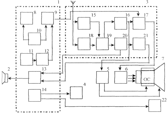
Figure 8.13. Block diagram of a TV type 4USTST
The signal processing module performs the following functions:
- amplification and selection of TV signals and their conversion into intermediate frequency signals;
- amplification of intermediate frequency image signals and decoding of image signals;
- decoding a full TV signal, generating and amplifying primary color signals;
- amplification of intermediate sound frequencies, decoding and amplification of audio signals;
- automatic white balance.
The signal processing module includes: a UHF channel selector 15, an intermediate frequency image amplifier 16, a color block 17, a meter range channel selector 18, a separation filter 19, a block for amplifying the intermediate frequency of the audio signal and frequency detection 20, a low frequency amplifier 21.
The high-frequency image and audio signals received by the antenna are sent to the corresponding channel selector. In TV receivers, high-frequency image signals f HF.IZ and audio signals f HF.ZV are jointly amplified in signal selectors, each of which consists of a high-frequency amplifier (UHF), a signal mixer and a local oscillator. After passing through UHF, the signals f HF.IZ and f HF.ZV enter the mixer. The local oscillator frequency f GET is selected higher than the signal frequency. Therefore, signals of intermediate frequencies of image f IF.IZ and sound f IF.IZ of the following ratings are generated at the output of the mixer: f GET -f HF.IZ =f IF.IZ =38 MHz; f GET -f RF.ZV = f IF.ZV =31.5 MHz.
The newest TV models adopt a two-channel design of the intermediate frequency amplification path. To do this, the channel selector, which has a symmetrical output, is loaded onto a surface acoustic wave (SAW) filter, which has a special tap for a block to amplify the intermediate frequency of the audio signal. This separation filter can significantly improve the quality of sound by reducing the level of interference in the audio path.
To decode and generate video signals of primary colors (E R ", E 1 G, E " B), a color block consisting of a PAL decoder and a SECAM-PAL transcoder is used. The transcoder identifies signals transmitted via PAL and SECAM systems. When SECAM signals are received, they are converted into PAL signals. In this case, the demodulation of these signals and the conversion of color difference signals into primary color signals are carried out in the PAL decoder. In the case of direct reception of a PAL system signal, it is decoded only by the PAL decoder, and the transcoder does not take part in their processing.
The power module is made according to the circuit of a switching power supply. Therefore, there is no power transformer in it, and the voltage of the AC electrical network is converted into a sequence of pulses with a frequency of 1640 kHz. The DC voltage generated after rectification of these pulses is highly stable. This allows you to maintain the functionality of the TV when the AC mains voltage fluctuates within 176-242 V. The rectified mains voltage is transformed using a pulse transformer into the secondary voltages necessary for the TV to operate. After rectifying the secondary voltages, the power module produces the following output voltages: 150, 15, 12 and 8 V. The power module provides protection against short circuits in secondary circuits. Efficiency The power supply module has a value of at least 80%.
The scan module consists of horizontal and vertical scan generators. The horizontal scan generator includes a pre-amplifier, an output stage, and a TV raster correction device designed to eliminate geometric distortions of vertical lines and stabilize the horizontal size. In the horizontal scan generator, voltages are generated to power the anode, focusing and accelerating electrodes of the kinescope, which are created using a voltage multiplier. In addition, a 220V voltage is generated in the horizontal scan generator to power the output amplifiers for primary color signals. The frame scan generator includes: a master oscillator, a CGI shaper, devices for adjusting the size and linearity of the TV raster, a pre-amplifier, an output stage and a reverse pulse generator.
Fifth generation televisions (model 5USTST) are made on analog-digital integrated circuits with microprocessor control. As a result, 5USTST TVs differ from previous models in higher color image quality, a greater number of functionality and ease of operation. The microcomputer included in the TV provides automatic tuning to any TV radio channel in the meter and decimeter wavelength ranges, storing 90 parameters from selected programs, switching them in a ring towards increasing or decreasing the channel number, and their direct selection. In addition, fifth-generation TVs automatically switch to receive TV signals from various color TV systems, electronically adjust volume, brightness, contrast, saturation, remember their levels, switch to standby mode when the output signal disappears or after a preset timer has expired. A mandatory attachment for the 5USCT series TV is a wireless remote control.
The block diagram of one of the fifth generation TV models is shown in Figure 8.14. This TV design uses both analog and digital TV signal processing. The functions of the local oscillator in the channel selector are performed by a digital frequency synthesizer, and the color block is implemented using elements of digital technology. Most of the components and blocks of a color TV that require adjustment and configuration both during production and during operation are controlled and diagnosed by a microcomputer via a two-wire bus in accordance with a program recorded in the read-only memory (ROM) of the microcomputer. Instead of controls (usually touch or push-button switches and variable resistors), fifth-generation TVs use a functional keyboard (FC), with which you can configure and adjust the TV receiver.
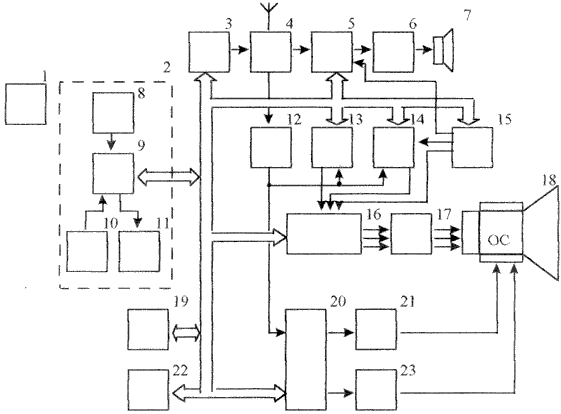
1- remote control, 2- control unit, 3- channel selector controller, 4 - channel selector, 5 - audio channel, 6 - low-frequency amplifier, 7 - acoustic system, 8 - remote control system, 9 - microcomputer, 10 - functional keyboard, 11 - indicator panel, 12 - IF image, 13 - color channel, 14 - Teletext decoder, 15 - external signal switch, 16 - video signal switch, 17 - kinescope board, 18 - color kinescope with deflection system, 19 - service switch adapter, 20 - synchro processor, 21 - vertical scan generator, 22 - power supply, 23 - line scan generator.
Figure 8.14. Block diagram of an analog-digital color TV
The TV microcomputer via a two-wire bus controls two sound processors (stereophonic sound option) and a synchro processor, signal switches and color decoders and the Teletext system. The possibility of control is provided both from the remote control (RC) and the built-in FC panel. IN modern TVs the main blocks controlled by a microcomputer via a digital bus are analog. Therefore, each controlled microcircuit contains a digital-to-analog converter (DAC) to create analog control signals.
The considered design of an analog-digital TV receiver is a transitional model to color digital TVs.
In promising fifth-generation TV models, it is planned to use a digital video processor and radio processor and a digital memory unit per frame of TV image. Moreover, at the inputs of digital processors, it is supposed to convert analog TV signals and audio signals received via the TV broadcasting system into digital form using an ADC. In this case, in the video processor, brightness and color signals will be isolated and processed from the full TV signal using digital filtering implemented by time delay, summation and multiplication circuits. Audio signals must be processed in a radio processor, where they are separated and formed. Volume and timbre adjustments, automatic recognition of mono- and stereophonic signals, as well as two-speech audio signals will also be carried out here. For monaural signals, it is possible to create a pseudo-stereo effect.
In 1997 Russian Federation government programs have been adopted to support the production of competitive domestic new generation televisions. The concept of building these TVs primarily involves:
- ensuring high quality image and sound in the SECAM-III standard as a result of optimization of radio and video paths and the use of modern picture tubes;
- achieving high manufacturability through the use of modern components with a high degree of integration;
- expansion of functionality (for example, implementation of freeze-frame functions, multi-screen, elimination of interline flicker, doubling the frequency of beams);
- modern TV control software;
- creating a TV with different picture tubes and functionality based on one chassis;
- development of modern design.
For a row foreign countries A characteristic feature is the rapid growth in the production of flat-screen TVs on plasma and liquid crystal (LCD) panels. For example, in Japan last years LCD TVs make up about 20% of the total number of color TVs produced.
Questions for self-control8.1. Explain the basic principles of transmitting TV signals over a radio channel.
8.2. How is the audio signal transmitted in a TV system?
8.3. Name the main elements of the block diagram of TV systems.
8.4. Formulate the basic principles for constructing joint analogue color television systems.
8.5. Name the most important features of SECAM-III color television systems.
8.6. Draw a block diagram of the encoder of the SECAM-III system.
8.7. For what purpose does the SECAM-III system introduce pre-emphasis on color difference signals before they are transmitted over a communication channel?
8.8. Draw the block diagram of the SECAM-III receiving decoding device.
8.9. List the main features of NTSC color television systems.
8.10. Give general characteristics PAL color television systems.
8.11. What are the design features of modern TV receivers?
8.1. Television / Ed. V.E. Jaconii.- M.: Radio and Communications, 1997.- 640 p.
8.2. Novakovsky S.V. Standard color television systems. - M.: Svyaz, 1976. - 267 p.
8.3. Khokhlov B.N. Decoding devices for color televisions. - M.: Radio and Communications, 1992. - 368 p.
8.4. Elyashkevich S.A., Peskin A.E. New generation televisions: Directory. - M.: MP "Symbol-R", 1996. - 216 p.
Send your good work in the knowledge base is simple. Use the form below
Students, graduate students, young scientists who use the knowledge base in their studies and work will be very grateful to you.
Siberian State University Telecommunications and Computer Science
Khabarovsk branch
COURSE PROJECT
by discipline
Radio receiving devices
Subject: “ Petelevision broadcast editor”
Developed by: Art. gr. XP - 61 Korolev I.E.
Cipher:06013ХР
Checked:teacher Yakovenko K. A.
Khabarovsk
2009
Course project assignment
Introduction
1. Drawing up a block diagram of the transmitter
1.2 Exciter selection
1.3 Selecting the type of amplification element
2. Development of a transmitter circuit diagram
Conclusion
Application
Application
Bibliography
ASSIGNMENT FOR A COURSE PROJECT.
Purpose of the transmitter………………………………………..TLV broadcasting
Oscillatory power in the antenna, kW…………………………………….4
TV channel……………………………………………………….5
Covered frequency range, MHz……………………………...92 - 100
Carrier frequency, MHz……………………………………………………93.25
Carrier frequency instability, Hz, no more than………………………...±100
Power ratio Riz/Rzv………………………………………….10: 1
Power consumption in quenching level transmission mode, kW,
no more………………………………………………………………………………….20
Power factor not less than……………………………………...0.92
Level of spurious emissions in the output signal, mW, no more than…….…1
Instability of the extinction level, %, no more than…………………………..±2.5
Signal-background ratio, dB, not less…………………………………….42
INTRODUCTION
Currently, third generation radio and television transmitting stations are in operation. They differ from previous generation stations in a number of fundamental features related to their purpose in the transmission network. First of all, it should be noted the main purpose of these stations is the creation of TV broadcast programs in areas already covered by single-program broadcasting. The installation of new equipment at these points should not lead to a proportional increase in the number of maintenance personnel, and the workload of existing personnel should increase slightly. All this is possible only with high reliability of the equipment, which ensures maintenance-free stable operation of the station for several months with the ability to control it remotely from the remote control of an already operating station. Secondly, the fundamental design of these stations must guarantee, during the specified time of unattended operation, stability and a high level of all quality indicators necessary for transmitting DTV signals. Based on this, it is customary to build stations that use:
transistor and micromodule technology in core process equipment to the maximum extent;
no more than one or two electric vacuum devices in the most powerful stages of the amplifier for modulated oscillations of the image and sound channels;
a basic low-power unit with the formation of a radio image signal (sound), which determines all the main quality indicators of the radio-television transmitting station as a whole;
block redundancy of preliminary paths and loaded redundancy of final power amplifiers.
The last two features are inherent in domestic stations, which use the formation of radio signals with an inverted spectrum in the intermediate frequency path, as well as the traditional quadrature scheme for adding the power of blocks in one semi-set. Thus, an ATRS station - 5/0.5 kW can operate in any of the radio channels of 1,2 or 3 TV bands, while in second generation stations this was impossible.
The first two features of the construction of third-generation stations should be discussed in some detail. In ATRS type stations, the transistor path provides a power level of 20 W. In the image channel, amplification from a power level of 1 W is produced by a three-stage linear amplifier, followed by two stages on tetrodes. There is only one tube unit in the audio channel. These features made it possible to dramatically reduce the size of the entire station. The power consumed from the network is also significantly reduced, which in the transmission mode of the damping level does not exceed 20 kW with a power gain of at least 0.92.
1. SOSTBLOCK DIAGRAM EVENTS
According to the assignment, a television image transmitter for the fifth TV channel with an output power of 4 kW is designed.
To increase equipment reliability, constant loaded redundancy is used. In this case, the transmitter is built on two identical half-sets, the powers of which are added using a bridge circuit. Semi-kits are completely autonomous. If one of them fails, the power addition bridge is bypassed, and the operating half-set is connected to the antenna-feeder path. The output stage of each half-set is built according to a quadrature circuit, which provides suppression of antenna echo, leading to distortions such as additional contours in the received image.
Currently received wide application intermediate frequency modulation, carried out using ring balanced modulators at low power levels. Modulation on the IF makes it possible to obtain higher quality indicators, but its use is only advisable when installing amplification of modulated oscillations of electric vacuum devices with high power amplification in the output stages.
Quartz oscillators with a frequency of 40 - 100 MHz are used as an exciter in the image transmitter, followed by multiplication if necessary. A special harmonic suppression filter is installed at the transmitter output, providing harmonic suppression up to 60 dB.
A television station includes an image and sound transmitter, which operate on one common antenna, so a separation filter is required at the station output to ensure independent operation of the transmitters.
1.1 Determination of the number of cascades of the entire path
Since the transmitter consists of two half-sets, and the total power is 4 kW, we define the output power of the lamp of one half-set as:
R l = (R 1 max)/(2. z lane),
where: P 1 max - maximum power supplied by the lamp;
z lane - transmitter efficiency;
A factor of 2 in the denominator indicates that the transmitter consists of two half-sets.
R l = (R 1 max)/(2. z AC) = 2.5/(2. 0.8) = 1.563 kW
Knowing that a cascade in a single-ended circuit with a common cathode with a characteristic slope S = 80 - 100 mA/V provides a power gain Kp = 25 - 30, we determine the power that must be supplied to the input of the lamp to ensure its normal operation:
R in = R l / K = 1563 / 30 = 52.1 W
The output amplifier of the exciter develops a power of 20 - 25 W, therefore it is necessary to turn on another amplification stage on the lamp to ensure normal operation of the amplifier. Thus, each half-set will consist of two amplification stages on tubes. The power of the audio transmitter according to GOST should be 1/10 or 10 times less than the power of the image transmitter, therefore one amplification stage is sufficient in the audio transmitter.
1.2 Pathogen selection
The pathogen or basic block consists of several subblocks:
frequency generation block;
IF modulator;
video correction block;
up-converters of image and sound;
linear transistor amplifiers;
power supplies;
The frequency generation unit generates three frequencies: IF of the image channel f IF = 35.75 MHz; local oscillator frequency exceeding the carrier frequency of the transmission channel at f frequency converter, for a given channel 5 f g = 129 MHz; IF of the audio channel f IF = 29.25 MHz. To obtain stable generation, two crystal oscillator: one is tuned to the f frequency of the inverter, and the other to a frequency in the range from 42 to 65 MHz.
The voltage from the output of the first generator is supplied to the amplifier, and then to the IF modulator of the image channel. The voltage from the output of the second is supplied to the frequency quadrupler and through a bandpass filter to two up-converters of image and sound.
1.3 Selecting the type of window reinforcement elementfinal and final cascades
To ensure the specified power of the designed transmitter, the final stage will be performed on a GU-73B lamp, and the pre-terminal image and final audio stage will be performed on a GU-74B lamp.
Basic parameters of lamps
GU-73B:
Rated oscillatory power, kW……………………….2.5
Cutoff frequency, MHz…………………………………………….250
Maximum anode current in pulse mode, no more, A………...8
Maximum anode voltage, kV……………………………2.1
Maximum voltage of the shielding mesh, V………………...300
Characteristic slope, mA/V……………………………………110
Filament voltage, V…………………………………………………...27
Filament current, A………………………………………………………4.6
Output capacitance, pF……………………………………………………………..27
Input capacitance, pF…………………………………………………...190
Pass-through capacitance, pF…………………………………………………0.2
Allowable power dissipation on the control grid, W…………5
Allowable power dissipation at the anode, kW…………………...2.5
Allowable power dissipation on the shielding mesh, W………35
GU-74B:
Rated oscillatory power, kW………………………...0.55
Cutoff frequency, MHz………………………………………………...60
Maximum anode current in pulse mode, no more than, A………2.4
Maximum anode voltage, kV…………………………………0.9
Maximum voltage of the shielding mesh, V………………...250
Characteristic slope, mA/V………………………………………..40
Filament voltage, V……………………………………………………………12.6
Filament current, A………………………………………………………3.6
Output capacitance, pF…………………………………………………..11
Input capacitance, pF…………………………………………………….51
Pass-through capacitance, pF…………………………………………………………..0.09
Allowable power dissipation on the control grid, W……….3.5
Allowable power dissipation at the anode, kW…………………...0.6
Allowable power dissipation on the shielding mesh, W………18
2. P DEVELOPMENTBASIC DIAGRAM OF THE TRANSMITTER
The image channel of the semi-set consists of two lamp stages on GU-74B and GU-73B lamps, as well as a resonator system for forming the frequency response, consisting of coaxial structures. The audio channel of the semi-set contains one tube stage on the GU-74B, almost completely similar to the first stage of the image channel. The cascades on the GU-74B are made according to a scheme with a common cathode. The input circuits, due to the low input impedance of the cascades, have sufficient broadband and do not affect the total frequency response of the power amplifier.
Anode loop systems of coaxial design are tuned to the average frequency of the transmission channel by capacitive plungers L a1 and L a3. The tuning elements E 1 and E 3 serve to slightly adjust the circuit when changing the lamp, and the elements E st provide communication with the output load circuit.
The cascade on the GU-73B is made according to a scheme with a common grid. The input circuit, low-resistance for a cascade with a common grid at point B, is recalculated through a piece of cable long? 1 at point A to a resistance close to 75 Ohms, which ensures normal load of the GU-74B circuit system. A choke in the cathode is included to pass the cathode current to the housing. The anode circuit of the GU-73B includes a complex circuit system consisting of an anode circuit and additional elements. The anode circuit is a coaxial structure into which the lamp is inserted. It is tuned to the average frequency of the transmission channel using a short-circuited plunger L a2. Adjustment element E 2 is used to slightly adjust the circuit when changing the lamp. By element E sv2 the anode circuit is connected to the output rigid feeder. On distance? 2 ~ l av / 4 from the anode circuit, tuned to fiz - (3.5 - 4.5) MHz and fiz + (8 - 9) MHz using tuning elements E 4 and E 5 brought out.
At the indicated frequencies, resonant circuits create short circuit at HF, and at the middle frequency of the channel they represent a circuit with high resistance.
The input grid devices of the lamp units are arranged in removable shielded units on coaxial anode structures and are equipped with electrical and mechanical interlocks.
Modulator
The modulator circuit is a balanced mixer assembled on diodes D1 - D4, connected to external circuits through matching RF transformers Tr1 (1:4) and Tr2 (4:1).
The modulator is integral part a boost converter unit, which, in addition to the balanced mixer, includes: IF and local oscillator input circuits; selection filter useful product F1 transformations; power amplifier up to a level of 20 W on transistors T5 - T9. The IF input circuit includes: a level regulator, a low-pass filter of k-type links, an amplifier on T1 and a heterodyne frequency suppression filter in the IF signal supply circuit.
The ring balanced mixer is assembled on four 2A104A diodes with resistors connected in series, which linearize the characteristic and reduce the influence of the spread of diode parameters. Filter F1 is a five-section frequency-symmetrical filter with 2f frequency suppression of at least 20 dB.
The output linear transistor amplifier is made using KT930A and KT930B transistors. The amplifier is two-stage with matching transformers at the input (16:1), between stages (4:1) and at the output (1:16). The transistors operate in class B mode; thermal stabilization boards are included in the base circuits.
CONCLUSION
In this course project, we developed a block diagram, a circuit diagram and made an electrical calculation of a television image transmitter of channel 5 TLV with an output power of 4 kW. All calculated parameters of this transmitter comply with the standards established in the assignment for the course project.
BIBLIOGRAPHY
Ivanov V.K. Equipment for radio and television transmitting stations. - M.: VZEIS, 1986.
Pirogov A. A. Television radio transmitters. - M.: VZEIS, 1968.
Shakhgildyan V.V. Radio transmitting devices. - M.: “Radio and Communication”, 1990.
Shakhgildyan V.V. Design of radio transmitting devices. - M.: “Radio and Communication”, 1984.
ANNEX 1
Pathogen 1
to amplifiers
1 and 2 semi-
sets
Input to amplifiers
PCTS
1 and 2 semi-
sets
to amplifiers
1 and 2 semi-
sets
Rice.
Block diagram of the exciter.
BVK - video correction unit
MUF - IF modulator
LTU - linear transistor amplifier
BFC - frequency generation block
BVL - block of input lines
APPENDIX 2
Amplifiers of the first half-set At the AFU
Block diagram of the transmitter.
UPO - pre-terminal amplifier
UOK - final amplifier
FG - harmonic filter
RF - separation filter
Ultrasound - sound amplifier
MS - addition bridge
PPI - image upconverter
PPZ - step-up audio converter
Similar documents
Selection of the block diagram of the first stages of the preselector, frequency conversion numbers. Determining the number of ranges. Calculation of mixer, parameters electronic devices, detector with amplitude limiter, end-to-end bandwidth of a television receiver.
course work, added 03/11/2014
Selecting the frequency modulation method. Calculation of a transistor oscillator based on a three-point point. Selection of exciter block diagram. Electrical calculation of transmitter path cascade modes. Design of a wide-range output communication circuit.
course work, added 03/29/2014
Development of a block diagram of a transmitter with basic modulation, the number of power amplification stages, final stage, transistor input circuit, quartz self-oscillator, emitter follower. Equivalent input resistance and capacitance of the transistor.
course work, added 07/17/2010
The procedure for drawing up a block diagram of a transmitter operating at 120 MHz. Selection and justification of a transistor for operation in the output stage. Calculation of the modulator and collector circuit. Calculation of parameters of the exciter, circuit multiplier and pre-final stage.
course work, added 01/03/2010
Calculation of the final stage of the transmitter and the matching circuit with the antenna. Drawing up a block diagram of the RPU. Selection of the transmitter block diagram and transistor for the transmitter output stage. Calculation of collector and base circuits, antennas, coil parameters.
course work, added 04/24/2009
Composition of the receiver block diagram. Determination of the input signal level, number of subbands, bandwidth, noise figure, parameters of selective systems of the radio frequency path. Development of an amplification path for the intermediate frequency of image and sound.
course work, added 10/30/2013
Calculation of the amplifier block diagram. Determination of the number of cascades. Distribution of distortions across cascades. Calculation of the final stage. Transistor selection. Calculation of preliminary stages. Calculation of an amplifier in the low frequency region (long times).
course work, added 11/19/2003
Choosing a block diagram of a radio receiver. Frequency range division. Calculation of the receiver linear path bandwidth. Selection of the first stages that provide the required receiver sensitivity. Design of a circuit diagram.
course work, added 08/30/2011
The use of synchronous radio broadcasting networks to increase the efficiency of transmitters and improve the audibility of radio broadcasts at low and medium frequencies. Development of a block diagram of the transmitter. Selecting an amplification element in the output stage.
course work, added 08/07/2009
Designing a block diagram of an amplification device audio frequencies. Drawing up schematic electrical diagrams and calculating the main parameters of the amplitude-frequency characteristics regulator, final and pre-terminal cascades.
In my youth, there was a period in my life - serving in the army “at the ends of the Earth”. This place was where steam locomotives did not go, ships visited once a year, and planes flew over our heads along an air corridor provided by the glorious and formidable (at that time) air defense system, vigilantly monitoring the crossing aircraft state border of our Motherland. The most “representative” of our friends were dogs, and among our neighbors were polar bears, deer, walruses and whales. There we had only one television program, received by a satellite dish called "Moscow".
Officers and warrant officers at that time had video recorders, and when they returned from summer vacations, they carried countless videotapes with films. These cassettes were then passed around until they became unusable. The most effective video recorder that spoils video cassettes was in our barracks. The front panel was missing and the recording mode lock did not work. And everyone was too lazy to press the bare micro buttons, trying to play or rewind. Often, instead of the required button, the record button was pressed, and a part of the film was simply erased. After such abuse at the cinema, the officers stopped giving videotapes to the barracks. To “meet the demand” of my comrades, I assembled a simple television transmitter, which broadcast a full-fledged television signal using VIDEO and AUDIO signals. The power was low, but within a radius of 100 meters there was reliable reception on the second television channel. This was enough to broadcast films to the entire town. The broadcast was made from one video recorder “at the request of telephone requests” from residents of the town.
The television transmitter described in this background requires an RF permit, so I will not publish its circuit diagram. Modern VCRs have the ability to connect to a display device (TV) through special connectors (via HF or LF channels). In some cases, it can be extremely inconvenient to use connecting cables to play a video on a TV. The proposed circuit allows you to amplify the power high frequency signal, generated by a video recorder and broadcast it over the air to remote consumers.
The operating radius of the device, which maintains guaranteed high image quality, is 50...60 m without taking into account attenuation (for example, a solid reinforced concrete wall of a house reduces its operating radius by 8...10 m). The circuit is powered from any stabilized source with a voltage of +9...18 V (recommended voltage value 12 V). The device operates in the frequency range 300...600 MHz.
;The schematic electrical diagram of the device is shown in the figure. 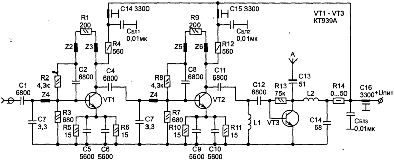
Transistors VT1 and VT2 assemble two stages of an RF amplifier with negative feedback (R-type). The total gain of both stages is 20 dB. Transistor VT3 is the final stage of the power amplifier. The gain of this stage is 6...7 dB.
The low noise level of the entire circuit (0.4...0.8 dB) with a total gain of at least 2.6 dB is ensured by the use of negative feedback on strip elements, which also eliminates self-excitation of amplifier stages and signal distortion.
The absence of adjustment elements makes the design accessible for repetition and eliminates difficulties when setting up high-frequency stages. The printed circuit board and the arrangement of elements on the board are shown in the figure below. 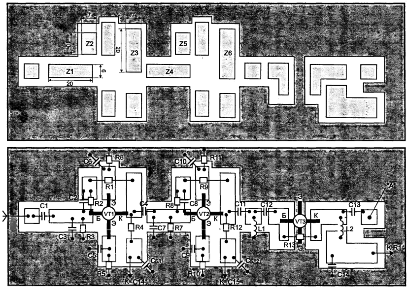
The board is made of double-sided foil fiberglass. The housing pads of both sides of the board should be connected to each other with through solder jumpers (1 jumper is installed on approximately 2 cm 2 of the board).
Holes for the terminals of structural elements are not needed. Between the cascades of the device, it is necessary to install shielding partitions connected to the circuit housing. It is advisable to supply power to the cascades through feedthrough capacitors installed in the holes of the shielding partitions with a capacity of 1000...3000 pF.
It is not advisable to maintain the printed conductors of the board; solder should only be in the places where radio elements are installed. Before installing elements on the board, it must be sanded with fine-grained sandpaper and then polished with a polishing paste (for example, GOI). It is advisable to use leadless passive elements for surface mounting. To ensure the above electrical parameters, it is necessary to accurately copy the printed circuit board and follow all recommendations.
The device uses powerful KT939A microwave transistors. Good results are obtained by using other transistors with similar parameters with a cutoff frequency of about 1 GHz, for example, KT610A and KT916A.
Coils L1, L2 are frameless and contain, respectively, 5 and 10 turns of enameled wire with a diameter of 0.3 mm. The inner diameter of both coils is 4 mm.
The antenna of the device is an aluminum or copper pin with a diameter of 10 mm and a length of 120 mm, soldered directly to the board at point “A” (see figure). The recommended antenna dimensions are given for channel 37 of the UHF range (600 MHz). This is the average frequency of any VCR RF output.
However, to increase the transmission range, without increasing the power of the signal amplifier, you can make an antenna consisting of two half-wave vibrators standing crosswise with a signal phase shift of 90 degrees. Thus, we will get a high-quality transmitting antenna with horizontal polarization and a circular radiation pattern. This is exactly the antenna I used in my first television transmitter. The transmission range is guaranteed to triple.
After assembly, the device is placed in a housing made of conductive material (for example, copper), which is connected around the perimeter by soldering to the housing pads of the board on both sides.
The device is connected with a coaxial cable directly to the high-frequency output of the VCR. An indoor UHF antenna is connected to the TV, and by changing its location it is adjusted according to best quality reception. If the distance between the device and the TV is small (5...6 m), the antenna is replaced with a piece of wire 10...15 mm long.
The utility model relates to communication technology, namely to digital transmitters for digital broadcasting in the DVD-T/H or DVD-T2 standard. The purpose of the utility model is to improve the design of the transmitter and is achieved due to the fact that the shaper has a demodulator input, an information input and service inputs for synchronization, power and control, the signal output of the shaper is connected to the input of the bandpass filter, and the control output is connected to the input of the demodulator, to which the output of the bandpass filter and the output of the antenna-feeder device are connected; The shaper is made in the form of a block that contains a modulator block, the signal output of which is connected to the input of the power amplifier block, the signal output of which is the signal output of the shaper, and the information output of the modulator block has feedback with an interface for input and presentation of data, the modulator block and the power amplifier block have feedback from the automation board, in addition, the outputs of the automation board are connected to the corresponding inputs of the modulator and power amplifier power supplies, the power supply outputs are connected to the corresponding inputs of the modulator block and the power amplifier block ; The transmitter contains a control unit made in the form of a single-board microcomputer. Positive effects include structural simplification of the television transmitter, increased service life, reduced weight and dimensions, and increased ease of use.
The utility model relates to communication technology, namely to digital transmitters for digital broadcasting in the DVB-T/H or DVB-T2 standard.
A transmitter for digital television is known from the existing state of the art [magazine “Broadcasting. Television and radio broadcasting", 8, 2006], containing a series-connected modulator, exciter, power amplifier, bandpass filter and antenna-feeder device (AFD).
The main disadvantage of the known transmitter is the inability to remotely control the operating parameters of the transmitter, as well as low stability of operation due to the lack of a cooling system or heat removal from the power amplifier.
The closest in technical essence is the Polaris TVC television transmitter from NPP Triada-TV LLC, consisting of a signal conditioner capable of encoding, modulating and converting the carrier frequency of the signal, as well as a power amplifier, a remote control unit and a bandpass filter, which adapted for placement in a 19" server rack. To cool the air, a cooling system is installed in the immediate vicinity of the rack.
The disadvantage of the prototype is the impossibility of remote control and monitoring of operation without turning on an additional monitoring system, which increases the overall dimensions of the transmitter, reducing its reliability and manufacturing costs in general. Another disadvantage is the high heat generation due to the fact that the functional units are made in the form of separate blocks with a large total power consumption, which leads to an increase in the air temperature in the working room and negatively affects the stability of operation and service life. These disadvantages are due to the imperfect design of the television transmitter.
The purpose of the utility model is to improve the design of the transmitter.
The technical result of the claimed utility model is to improve performance, reduce the size of the transmitter and increase stability.
The technical result lies in the fact that a television transmitter containing a signal conditioner, a power amplifier, a remote control unit and a bandpass filter, characterized in that the shaper has a demodulator input, an information input and service inputs for synchronization, power and control, the signal output of the shaper is connected to the input of the bandpass filter, and the control output is connected to the input of the demodulator, to which the output of the bandpass filter and the output of the antenna-feeder device are connected; The shaper is made in the form of a block that contains a modulator block, the signal output of which is connected to the input of the power amplifier block, the signal output of which is the signal output of the shaper, and the information output of the modulator block has feedback to the data input and presentation interface, the modulator block and the power amplifier block have feedback with the automation board, in addition, the outputs of the automation board are connected to the corresponding inputs of the modulator and power amplifier power supplies, the power supply outputs are connected to the corresponding inputs of the modulator block and the power amplifier block; The transmitter contains a control unit made in the form of a single-board microcomputer. The modulator unit contains a remote control unit made in the form of a single-board microcomputer.
In particular, the computer of the modulator unit is equipped with two Ethernet controllers, USB, COM, VGA ports for connecting additional external devices. The computer software is located on an internal flash drive and is a set of programs in languages high level running under Linux OS. It is possible to quickly update the software, both from the drive and remotely.
In particular, the power amplifier unit contains two fans configured to remove generated heat.
In particular, on the front panel of the driver there is a panel LED indication, which is connected to the automation board.
In particular, the automation board is designed to control and monitor the operation of the driver.
In particular, the interface for entering and presenting data (former) of the transmitter is made in the form of a touch display.
Brief description of drawings
In fig. 1 presented structural scheme television transmitter.
In fig. Figure 2 shows the functional diagram of the driver.
In fig. Figure 3 shows a block diagram of the modulator block.
In fig. Figure 4 shows a block diagram of a power amplifier according to the 1st implementation option.
In fig. Figure 5 shows a block diagram of a power amplifier according to the 2nd implementation option.
In fig. Figure 6 shows a block diagram of a power amplifier according to the 3rd implementation option.
In fig. Figure 7 shows the relative arrangement of the blocks of the television transmitter.
In fig. 8a presented appearance prototype of a television transmitter.
In fig. Figure 8b shows the appearance of the rear panel of the former.
In fig. Figure 9 shows the location of the functional units and blocks of the driver.
Implementation of a utility model
Digital broadcast television transmitter(Fig. 1) consists of a series-connected shaper 1, a bandpass filter 3 and an AFU 3. The shaper 1 has a demodulator input D, an information input I, as well as service inputs for synchronization - C, control - and power A. The signal output S is connected to the input filter. The control output K, the output of the filter 2 and the output of the AFU 3 are connected to the input D of the driver 1.
Shaper 1 (Fig. 2) contains a modulator block 4, the signal output of which is connected to the input of the power amplifier block 5, the signal output of which is the signal output of the shaper 1. The information output of the modulator block 4 has feedback to the data input and presentation interface 6. The modulator block 4 and The power amplifier block 5 has feedback from the automation board 7. In addition, the power outputs of the board 7 are connected to the corresponding inputs of the power supplies of the modulator 8 and the power supply of the power amplifier 9. The outputs of the power supplies 8, 9 are connected to the corresponding power inputs of block 4 and block 5.
Shaper 1 has connectors ASI1/ASI2, IP1/IP2, 10M, 1PPS, GLONASS, LAN1/LAN2, USB0/USB1, Demodulator and Control, which are connected to the corresponding inputs of block 4. To connect an internal monitor (not shown in the drawing) to the output The VGA OUT connector has a VGA IN connector connected to the input of interface 6. The VGA connectors are located to provide the user with the ability to connect an external monitor. The user can also connect a mouse and keyboard via USB, a GPRS modem or a storage device. To the input connector Network connected to board 7 is connected electrical network 220 V. On the front panel of the driver 1 there is an indication panel 10 (Fig. 7) with the ability to control the operating modes of the driver 1.
The modulator block 4 (Fig. 3) contains a modulator 11, the signal output of which is connected to the backplane 12, the signal output of which is the signal output of the modulator block 4. The supply output of the backplane 12 is connected to the corresponding supply input of the backplane 13, to the supply outputs which connects the power inputs of the modulator 11, the demodulator 14 and the computer 15. In addition, the backplane 13 has feedback via the RS-232 interface and the universal serial bus with the modulator 11 and the computer 15, and only via the universal serial bus interface with the demodulator 14 Backplane 13 can only be used for convenience of switching and does not functionally ensure the achievement of the specified technical result. The computer communicates with the modulator via RS-232 and with the demodulator via USB, the remaining ports (1*RS-232, 2*USB, 2* Ethernet) are reserved for external user devices.
The modulator block 4 contains a fan 16 designed to remove heat from the modulator block 11 and the computer 15
The amplifier block 5 according to the first embodiment (Fig. 4) contains an adapter board 17, the supply input of which is connected to the corresponding supply output of the power supply 9, and the supply and signal outputs with the corresponding inputs of the variable attenuator 18, pre-amplifier 19 and output amplifier 20, connected each other sequentially. In addition, the signal outputs of the board 17 are connected to the display panel 10 of the driver 1.
The amplifier block 5 according to the second embodiment (Fig. 5), in addition to the first embodiment, contains an amplifier stage 21, the signal input of which is connected to the pre-amplifier 19, and the output to the corresponding input of the amplifier 20. In addition, block 5 contains a fan control board 22 supplying and the signal inputs of which are connected to the corresponding outputs of the board 17. The supply inputs of the fans 23 are connected to the corresponding outputs of the board 22.
The amplifier block 5 according to the third embodiment (Fig. 6), in contrast to the implementation according to the second embodiment, instead of an output amplifier 20, contains an output stage 24 containing a quadrature power amplifier, two power amplifiers and a quadrature power adder (not shown in the drawing).
Information input I of the driver 1 is configured to input a transport stream.
The former 1 can be made in the form of a block corresponding to a 19-inch rack standard with a height of 3U with the possibility of placement in a 19" cabinet.
The data input and presentation interface 6 is made in the form of a touch panel with the ability to control and monitor the operation of the shaper 1.
The computer 15 is made with the ability to change the modes and parameters of the modulator 4, the operating modes of the unit 5 via the universal serial bus USB4, organizing local and remote monitoring and control via the interface inputs LAN1/LAN2 and/or USB0/USB1 of the modulator 4, servicing interface 6 via the USB5 bus , also outputting information to external VGA monitor via VGA OUT.
The automation board 7 is made with the ability to turn on/off the driver 1 with a corresponding LED display of its status on the display panel 10, control the voltages and currents of voltage consumption, organize exchange with the computer 15 and control the cooling fans 23 of block 5.
As software shaper 1, you can use the “TeamCast” program.
The demodulator 14 is designed to measure and control the main characteristics of the shaper 1 with information output to the interface 6.
Bandpass filter 2 is designed to suppress out-of-band emissions (interference).
Bandpass filter 2 can be installed in close proximity to driver 1 and is connected to the output of driver 1 with a standard jumper.
AFU 3 (equivalent to an antenna) is connected to the output of filter 2.
The device works as follows.
Turning on the shaper
After turning on the driver 1 with the “Network” switch on the rear wall (driver status is off), the network voltage is supplied to board 7 and the LED on panel 10 turns on in red, which indicates that driver 1 is in the off state (status is off).
After pressing the button (the button must be held for 2 seconds), the red LED on panel 10 will begin to blink, i.e. The status of the driver is set to enabled. If within 3 seconds the mains voltage is normal (180 V< Сеть < 242 В), то на панели 10 начнет мигать зеленый светодиод и напряжение сети с платы 7 поступает на блоки питания 8, 9.
The 12 V voltage from the power supply 8 is supplied to block 4 to the backplane 13, then to the fan 16 and to the backplane 12. From the backplane 12, 12 V power is supplied to the modulator 11, the demodulator 14 and the computer 15. The modulator has its own non-volatile memory, where it stores the settings of the previous launch with which it starts, without waiting for the computer to load.
A voltage of 26/42/50 V from block 9 is supplied to block 5. Also, from block 9 through board 7, in the case of using the 2nd and 3rd amplifier designs, a voltage of 50 V is supplied to block 5.
If all voltages are normal, then block 5 is turned on. Approximately 15 seconds after block 8 is turned on, a high-frequency signal is supplied from block 4 to block 5, after which the output power of shaper 1 smoothly rises to the nominal level.
1.5 minutes after block 8 is turned on, computer 15 is loaded in block 4, which polls board 7. If board 7 is polled correctly, the green LED on panel 10 will turn on and an invitation to work will appear on interface 6 (or on the external display) .
Operation of a television transmitter.
The generated transport stream TS and synchronization signals are supplied to the inputs of shaper 1, where a high-frequency digital signal is generated on the selected television channel of the required output power, which is supplied to filter 2 and, then, to AFU 3.
Block 4 receives the generated transport stream at the ASI1/ASI2 or IP1/1P2 inputs, as well as, if necessary, 10M/1PPS or GLONASS synchronization signals. The generated digital television radio signal on the selected television channel is supplied to block 5 through backplane 13.
Modulator 4 is controlled via the RS-232 interface.
Demodulator 14 receives an external radio signal to measure:
Emission spectrum in a band up to 100 MHz with a step of 0.125 MHz;
Parameters on the selected digital television channel (MER, BER).
The automation board 7 controls the heat release power of the power amplifier unit 5 and, to regulate the air temperature, regulates the rotation speed of the fans 23 of the unit 5.
Changes in the operating modes of block 5 are carried out via the USB4 bus of block 4. The control signal from USB4 is supplied from backplane 13 to the USB/COM adapter, from which the RX and TX control signals via backplane 12 are sent to board 7, which changes the modes of block 5 .
Using the information displayed on interface 6 and the LED indication of panel 10, continuous monitoring of the operation of the transmitter is carried out.
Air exhaust (shown by arrows in Fig. 7) can be provided through the false panel of the former 1 and through a system of air ducts communicating with fans 23.
Warm air can be removed to another room or outside through external air ducts (not shown in the drawing). Remote control of the driver.
Remote control of the shaper is necessary for service personnel to quickly configure a television transmitter and monitor broadcast parameters.
The computer unit software provides the user with two options for remote control: via a web interface and via the SNMP protocol. The computer supports any available communication channels Ethernet, GPRS, ADSL. The security level of Linux OS also allows you to work through public networks and INTERNET.
The industrial applicability of the utility model is due to the fact that in 2013 the applicant produced a prototype (Fig. 8, Fig. 9) of a television transmitter and its tests practically confirmed the positive effects achieved.
Useful technical effects from using a utility model are:
constructive simplification of a television transmitter, which consists in the fact that the transmitter consists of two separate blocks of a shaper and a band-pass filter, which provide encoding, modulation, conversion of the carrier frequency of the signal, power amplification, remote control of the transmitter and suppression of out-of-band interference;
increased service life compared to the prototype, due to the fact that the cooling system is installed directly in the driver block and its use eliminates overheating of the component blocks of the driver;
reduction in weight and overall dimensions due to the fact that the main functional elements are placed in a single block;
simplifying troubleshooting and localization, increasing system reliability, due to the fact that the driver implements the ability to monitor operating modes and control all systems from a single display panel and interface
increasing ease of use by providing continuous monitoring and control of the transmitter using remote access.
As an additional positive effect, one can highlight the reduction of costs during operation of the transmitter and simplification of the design through the use of a local cooling system and the elimination of additional air and water cooling systems.
1. A television transmitter containing a signal conditioner, a power amplifier, a remote control unit and a bandpass filter, characterized in that the shaper has a demodulator input, an information input and service inputs for synchronization, power and control, the signal output of the shaper is connected to the input of the bandpass filter, and the control the output is connected to the input of the demodulator, to which the output of the bandpass filter and the output of the antenna-feeder device are connected; The shaper is made in the form of a block that contains a modulator block, the signal output of which is connected to the input of the power amplifier block, the signal output of which is the signal output of the shaper, and the information output of the modulator block has feedback to the data input and presentation interface, the modulator block and the power amplifier block have feedback with the automation board, in addition, the outputs of the automation board are connected to the corresponding inputs of the modulator and power amplifier power supplies, the power supply outputs are connected to the corresponding inputs of the modulator block and the power amplifier block; The transmitter contains a control unit made in the form of a single-board microcomputer.
2. The television transmitter according to claim 1, characterized in that the modulator unit contains a remote control unit made in the form of a single-board microcomputer.
3. The television transmitter according to claim 1, characterized in that the computer of the modulator unit is equipped with two Enternet controllers, USB, COM, VGN ports for connecting additional external devices.
4. A television transmitter according to claim 1, characterized in that the power amplifier unit contains two fans designed to remove generated heat.
5. The television transmitter according to claim 1, characterized in that on the front panel of the former there is an LED display panel, which is connected to the automation board.
6. The television transmitter according to claim 1, characterized in that the automation board is designed to control and monitor the operation of the driver.
7. The television transmitter according to claim 1, characterized in that the interface for input and presentation of data from the driver is made in the form of a touch display.
The TV modulator circuits published in amateur radio publications are not very convenient for repetition - they contain a large number of parts, the modulation is carried out in the self-oscillator stage. The circuit options described below are free from these disadvantages.
The circuit (Fig. 1) is “classical” according to the principles of Japanese circuit design: a small number of high-quality parts, adjustment is made by changing one or two parts. So as not to be frightened by the “simplicity” of the circuit, we note that the path to it and other circuits began with “anti-PTK” (I wanted to mount a device that transmits image and sound signals on any of the meter channels), then there were circuits with sealed cases and feed-through capacitors in the walls .
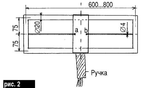 It turns out that the VHF circuit can be mounted without screens and without quartz frequency stabilization (the television receiver has an AFC system!), it is only important to position the parts correctly.
The coil contains 1+1+3 turns for the upper MV channels and two to three times more for the lower MV channels.
Modulation is carried out in a push-pull output stage using field-effect transistors VT2, VT3, taken from the same box and tested at least ohm
trom and milliammeter (current at operating voltage and “zero” gate). The video signal is supplied to the source circuit of the output transistors through filter R7, C5. Thus, amplitude negative modulation is realized.
The drains of the output transistors are directly connected to the elements of a triple loop vibrator made with high input resistance (Fig. 2). The vibrator resistance is more than 2 kOhm, so the transistors are connected in a consistent manner (without adjustment elements) to a resonant load.
To set up the device, it is important to know the general principles:
- a fiberglass board is mounted directly on the antenna, the “plus” circuits are connected to the midpoint of the antenna with screws through the board;
- the master oscillator coil is located on the axial (dotted line) line, it is oriented perpendicular to the plane of the antenna;
- The cable with the video signal goes along with the power cable also through the middle zone of the vibrator (there is a handle there, and you can even hold the antenna in one hand, the video camera in the other, the battery on your shoulder).
The initial frequency setting is carried out with a tuning capacitor C, then it is replaced with a constant capacitance, and by changing the dimensions of the coil L the final adjustment is made (in one of the copies of the modulator with the antenna of the 6th channel, the operating frequency was almost on the 7th channel, but the quality of transmission was pleased, and the adjustment was stopped). The circuit does not include a radio frequency cable to the antenna and a device for matching the transmitter with the cable and the cable with the antenna.
The master oscillator transistor is not very high-frequency; on the upper channels of the MV it can be replaced with a GT313B, given the smaller temperature range than that of silicon transistors. You can make a master oscillator on a field-effect transistor with an insulated gate and an induced p-channel. Figure 3 shows the circuits of the master oscillator at a higher supply voltage (Figure 3, a) and at a lower voltage (Figure 3, b). In the first case, you have to select the gate bias voltage so that the source current is not too large. In the second, select the location of the coil L so that the following conditions are met: the signal from the antenna is not induced into the circuit; the operating frequency would be with “average” coil dimensions (not very compressed and not very stretched); The microphone effect would be reduced - the influence of mechanical influences on the board on the generated frequency (in a video transmitter-only circuit this effect is not noticeable).
Compressing the coil turns increases its inductance and lowers the operating frequency, while stretching the turns increases the generation frequency. In any case, coils with fewer turns of relatively thick wire are preferable - this makes it easier to ensure stability of dimensions and circuit adjustment. At the beginning of the setup, you should use a thin flexible wire for the loop coil to make it easier to go through the initial stages of setup.
Important and human factor- if a couple field effect transistors you ruined it with the touch of your hand (static!), then leave the experiments for a while. To protect against static, it is convenient to tie all the terminals of the “field switch” together with tinned thin wire, folded in half (there are wire breakages when bending). After this, the leads of the transistor are unbent, the entire circuit is soldered, then the shorting wire is removed with a scalpel and tweezers (the operator firmly holds the “ground” of the board with his hand to prevent breakdown of the transistor gate).
It is good to install the circuits on one side of the foiled fiberglass laminate (the other side is a solid “mass”). It is convenient to fasten such a board with screws inside the cases of other devices. It should be taken into account that the antenna vibrator is connected to the “plus”, and do not allow the housing to be connected to the antenna. The sections of the board with potential “+” are secured to the antenna with screws.
Another difference between the diagram in Fig. 3 is a higher voltage of the high-frequency signal than in the circuit in Fig. 1.